2d materials electrical control of interlayer exciton dynamics in … · 2d materials electrical...
TRANSCRIPT
2D MATERIALS
Electrical control of interlayer exciton dynamicsin atomically thin heterostructuresLuis A. Jauregui1*, Andrew Y. Joe1, Kateryna Pistunova1, Dominik S. Wild1, Alexander A. High1,2,You Zhou1,2, Giovanni Scuri1, Kristiaan De Greve1,2†, Andrey Sushko1, Che-Hang Yu3‡,Takashi Taniguchi4, Kenji Watanabe4, Daniel J. Needleman3,5,6, Mikhail D. Lukin1,Hongkun Park1,2, Philip Kim1,3§
A van der Waals heterostructure built from atomically thin semiconducting transition metaldichalcogenides (TMDs) enables the formation of excitons from electrons and holes in distinct layers,producing interlayer excitons with large binding energy and a long lifetime. By employingheterostructures of monolayer TMDs, we realize optical and electrical generation of long-lived neutraland charged interlayer excitons. We demonstrate that neutral interlayer excitons can propagate acrossthe entire sample and that their propagation can be controlled by excitation power and gate electrodes.We also use devices with ohmic contacts to facilitate the drift motion of charged interlayer excitons.The electrical generation and control of excitons provide a route for achieving quantum manipulation ofbosonic composite particles with complete electrical tunability.
Long-lived excitons can be potentially usedfor the realization of coherent quantummany-body systems (1–3) or as quantuminformation carriers (4, 5). In conventionalsemiconductors, the exciton lifetime can
be increased by constructing double–quantumwell (DQW)heterostructures, inwhich spatiallyseparated electrons and holes form interlayerexcitons (IEs) across the quantumwells (6–12).Strongly bound IEs can also be formed bystacking two single atomic unit cells of tran-sition metal dichalcogenides (TMDs) into avan der Waals (vdW) heterostructure. TMDheterostructures, such as MoSe2/WSe2, MoS2/WS2, and MoS2/WSe2, have shown ultrafastcharge transfer (13), the formation of IEs witha large binding energy of ~150 meV (14), anddiffusion over long distances (15). Moreover,the tight binding and small exciton Bohr radiuspotentially allow for quantum degeneracy ofthese composite bosons, which may lead toexciton condensation at substantially elevatedtemperatures compared to those of, e.g., con-ventional Bose-Einstein condensates of coldatoms (2).In this work, we fabricate individually elec-
trically contacted optoelectronic devices usinghexagonal boron nitride (h-BN)–encapsulated
vdW heterostructures of MoSe2 and WSe2(16, 17). Optically transparent electrical gatesand ohmic electrical contacts realized for theindividual atomic layers allow us to have com-plete control of the carrier densities in eachTMD of the DQW while maintaining full op-tical access. The top and bottom insets of Fig. 1Ashow an optical image of a representative de-vice with false-colored top gates and a schematiccross section, respectively [a detailed devicescheme is illustrated in fig. S1 (18)]. The greenand red false-colored gates depict the contactgates for doping the MoSe2 and WSe2 regions,respectively. These contact gates, together withthe prefabricated Pt electrodes, provide ohmiccontacts in the WSe2 p-channel (19).The presence of the top (optically transpar-
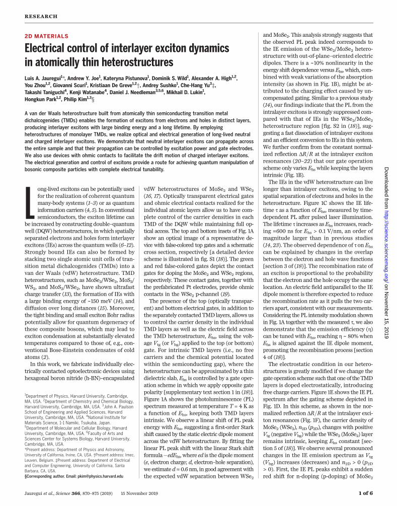
ent) and bottom electrical gates, in addition tothe separately contacted TMD layers, allows usto control the carrier density in the individualTMD layers as well as the electric field acrossthe TMD heterostructure, Ehs, using the volt-age Vtg (or Vbg) applied to the top (or bottom)gate. For intrinsic TMD layers (i.e., no freecarriers and the chemical potential locatedwithin the semiconducting gap), where theheterostructure can be approximated by a thindielectric slab, Ehs is controlled by a gate oper-ation scheme in which we apply opposite gatepolarity [supplementary text section 1 in (18)].Figure 1A shows the photoluminescence (PL)spectrummeasured at temperature T = 4 K asa function of Ehs, keeping both TMD layersintrinsic. We observe a linear shift of PL peakenergy with Ehs, suggesting a first-order Starkshift caused by the static electric dipolemomentacross the vdW heterostructure. By fitting thelinear PL peak shift with the linear Stark shiftformula�edEhs, where ed is the dipolemoment(e, electron charge; d, electron–hole separation),we estimate d≈ 0.6 nm, in good agreementwiththe expected vdW separation between WSe2
andMoSe2. This analysis strongly suggests thatthe observed PL peak indeed corresponds tothe IE emission of the WSe2/MoSe2 hetero-structure with out-of-plane–oriented electricdipoles. There is a ~10% nonlinearity in theenergy shift dependence versusEhs, which, com-bined with weak variations of the absorptionintensity (as shown in Fig. 1B), might be at-tributed to the charging effect caused by un-compensated gating. Similar to a previous study(14), our findings indicate that the PL from theintralayer excitons is strongly suppressed com-pared with that of IEs in the WSe2/MoSe2heterostructure region [fig. S2 in (18)], sug-gesting a fast dissociation of intralayer excitonsand an efficient conversion to IEs in this system.We further confirm from the constant normal-ized reflection DR=R at the intralayer excitonresonances (20–22) that our gate operationscheme only varies Ehs while keeping the layersintrinsic (Fig. 1B).The IEs in the vdW heterostructure can live
longer than intralayer excitons, owing to thespatial separation of electrons and holes in theheterostructure. Figure 1C shows the IE life-time t as a function of Ehs, measured by time-dependent PL after pulsed laser illumination.The lifetime t increases asEhs increases, reach-ing ≈600 ns for Ehs > 0.1 V/nm, an order ofmagnitude larger than in previous studies(14, 23). The observed dependence of t on Ehs
can be explained by changes in the overlapbetween the electron and hole wave functions[section 3 of (18)]. The recombination rate ofan exciton is proportional to the probabilitythat the electron and the hole occupy the samelocation. An electric field antiparallel to the IEdipolemoment is therefore expected to reducethe recombination rate as it pulls the two car-riers apart, consistentwith ourmeasurements.Considering the PL intensitymodulation shownin Fig. 1A together with the measured t, we alsodemonstrate that the emission efficiency (h)can be tuned with Ehs, reaching h ~ 80%whenEhs is aligned against the IE dipole moment,promoting the recombination process [section4 of (18)].The electrostatic condition in our hetero-
structures is greatly modified if we change thegate operation scheme such that one of theTMDlayers is doped electrostatically, introducingfree charge carriers. Figure 1E shows the IE PLspectrum after the gating scheme depicted inFig. 1D. In this scheme, as shown in the nor-malized reflection DR=R at the intralayer exci-ton resonances (Fig. 1F), the carrier density ofMoSe2 (WSe2), n2D (p2D), changes with positiveVtg (negativeVbg) while theWSe2 (MoSe2) layerremains intrinsic, keeping Ehs constant [sec-tion 5 of (18)]. We observe several pronouncedchanges in the IE emission spectrum as Vtg
(Vbg) increases (decreases) and n2D > 0 (p2D> 0). First, the IE PL peaks exhibit a suddenred shift for n-doping (p-doping) of MoSe2
RESEARCH
Jauregui et al., Science 366, 870–875 (2019) 15 November 2019 1 of 6
1Department of Physics, Harvard University, Cambridge,MA, USA. 2Department of Chemistry and Chemical Biology,Harvard University, Cambridge, MA, USA. 3John A. PaulsonSchool of Engineering and Applied Sciences, HarvardUniversity, Cambridge, MA, USA. 4National Institute forMaterials Science, 1-1 Namiki, Tsukuba, Japan.5Department of Molecular and Cellular Biology, HarvardUniversity, Cambridge, MA, USA. 6Faculty of Arts andSciences Center for Systems Biology, Harvard University,Cambridge, MA, USA.*Present address: Department of Physics and Astronomy,University of California, Irvine, CA, USA. †Present address: Imec,Leuven, Belgium. ‡Present address: Department of Electricaland Computer Engineering, University of California, SantaBarbara, CA, USA.§Corresponding author. Email: [email protected]
on Novem
ber 15, 2019
http://science.sciencemag.org/
Dow
nloaded from
(WSe2). Second, the PL peaks continuously red-shift as doping increases for both n- and p-sides. In this regime, Ehs is fixed (as discussedabove) and thus these shifts cannot be explainedby the Stark effect. Lastly, the PL intensity di-minishes rapidly as doping increases.Our measurements in the doped regime can
be explained by the formation of charged IEs(CIEs) (24). As shown in the normalized reflec-tion measured with the same gating scheme,we can identify (i) intrinsic/p, (ii) intrinsic/intrinsic, and (iii) n/intrinsic regions by thedisappearance of the absorption dips for intra-layer excitons in MoSe2 and WSe2 (25), whichare well aligned with the sudden red shiftobserved in IE PL (vertical dashed lines inFig. 1, D to G). Thus, this jump in energy canbe related to theCIEs.Note that chargedexcitonscan be referred to as trions (i.e., three-bodybound states) (26–29) or, alternatively, attract-ive polarons (i.e., excitonic states dressed bya polarized fermionic sea, similar to those in
monolayer TMDs) (30, 31). The value of theobserved jump ≈10 meV (15 meV) for positive(negative) CIEs is in good agreement with thecalculated binding energy of CIEs (24). Thelifetime of CIEs is ≈100 ns near the band edgebut decreases with increased doping, presum-ably owing to additional decay channels enabledby scattering with free carriers (Fig. 1G).We create high densities of IEs by increasing
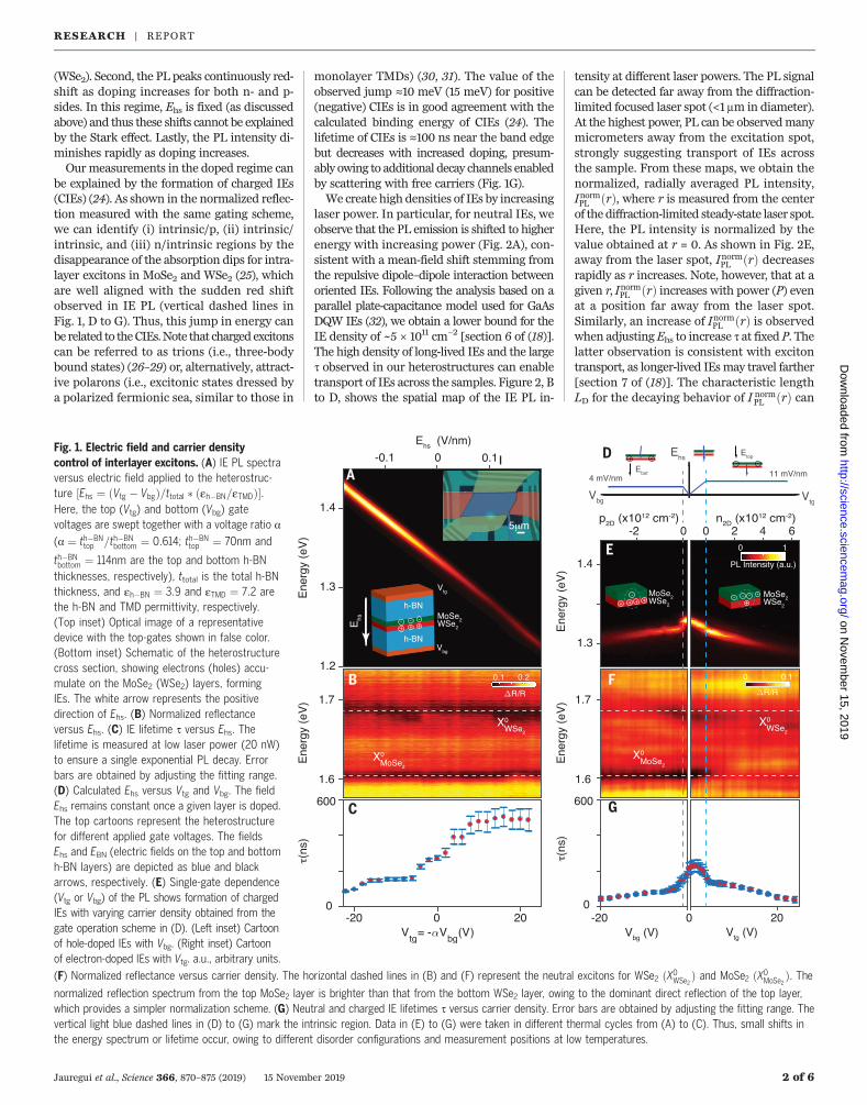
laser power. In particular, for neutral IEs, weobserve that the PL emission is shifted to higherenergy with increasing power (Fig. 2A), con-sistent with a mean-field shift stemming fromthe repulsive dipole–dipole interaction betweenoriented IEs. Following the analysis based on aparallel plate-capacitance model used for GaAsDQW IEs (32), we obtain a lower bound for theIE density of ~5 × 1011 cm−2 [section 6 of (18)].The high density of long-lived IEs and the larget observed in our heterostructures can enabletransport of IEs across the samples. Figure 2, Bto D, shows the spatial map of the IE PL in-
tensity at different laser powers. The PL signalcan be detected far away from the diffraction-limited focused laser spot (<1 mm in diameter).At the highest power, PL can be observedmanymicrometers away from the excitation spot,strongly suggesting transport of IEs acrossthe sample. From these maps, we obtain thenormalized, radially averaged PL intensity,InormPL ðrÞ, where r is measured from the centerof the diffraction-limited steady-state laser spot.Here, the PL intensity is normalized by thevalue obtained at r = 0. As shown in Fig. 2E,away from the laser spot, InormPL ðrÞ decreasesrapidly as r increases. Note, however, that at agiven r, InormPL ðrÞ increases with power (P) evenat a position far away from the laser spot.Similarly, an increase of InormPL ðrÞ is observedwhen adjustingEhs to increase t at fixed P. Thelatter observation is consistent with excitontransport, as longer-lived IEsmay travel farther[section 7 of (18)]. The characteristic lengthLD for the decaying behavior of I normPL ðrÞ can
Jauregui et al., Science 366, 870–875 (2019) 15 November 2019 2 of 6
Fig. 1. Electric field and carrier densitycontrol of interlayer excitons. (A) IE PL spectraversus electric field applied to the heterostruc-ture ½Ehs ¼ ðVtg � VbgÞ=ttotal � ðeh�BN=eTMDÞ�.Here, the top (Vtg) and bottom (Vbg) gatevoltages are swept together with a voltage ratio a
(a ¼ th�BNtop =th�BN
bottom ¼ 0:614; th�BNtop ¼ 70nm and
th�BNbottom ¼ 114nm are the top and bottom h-BNthicknesses, respectively), ttotal is the total h-BNthickness, and eh�BN ¼ 3:9 and eTMD ¼ 7:2 arethe h-BN and TMD permittivity, respectively.(Top inset) Optical image of a representativedevice with the top-gates shown in false color.(Bottom inset) Schematic of the heterostructurecross section, showing electrons (holes) accu-mulate on the MoSe2 (WSe2) layers, formingIEs. The white arrow represents the positivedirection of Ehs. (B) Normalized reflectanceversus Ehs. (C) IE lifetime t versus Ehs. Thelifetime is measured at low laser power (20 nW)to ensure a single exponential PL decay. Errorbars are obtained by adjusting the fitting range.(D) Calculated Ehs versus Vtg and Vbg. The fieldEhs remains constant once a given layer is doped.The top cartoons represent the heterostructurefor different applied gate voltages. The fieldsEhs and EBN (electric fields on the top and bottomh-BN layers) are depicted as blue and blackarrows, respectively. (E) Single-gate dependence(Vtg or Vbg) of the PL shows formation of chargedIEs with varying carrier density obtained from thegate operation scheme in (D). (Left inset) Cartoonof hole-doped IEs with Vbg. (Right inset) Cartoonof electron-doped IEs with Vtg. a.u., arbitrary units.
(F) Normalized reflectance versus carrier density. The horizontal dashed lines in (B) and (F) represent the neutral excitons for WSe2 ðX0WSe2Þ and MoSe2 ðX0MoSe2 Þ. The
normalized reflection spectrum from the top MoSe2 layer is brighter than that from the bottom WSe2 layer, owing to the dominant direct reflection of the top layer,which provides a simpler normalization scheme. (G) Neutral and charged IE lifetimes t versus carrier density. Error bars are obtained by adjusting the fitting range. Thevertical light blue dashed lines in (D) to (G) mark the intrinsic region. Data in (E) to (G) were taken in different thermal cycles from (A) to (C). Thus, small shifts inthe energy spectrum or lifetime occur, owing to different disorder configurations and measurement positions at low temperatures.
RESEARCH | REPORTon N
ovember 15, 2019
http://science.sciencem
ag.org/D
ownloaded from
be obtained from fitting e�r=LD=ffiffiffiffiffiffiffiffiffiffiffir=LD
pto
InormPL ðrÞ away from the laser excitation spot(dashed lines in Fig. 2E), following the two-dimensional diffusion model with a pointsource [section 8 in (18)]. As shown on the leftaxis of Fig. 2G, we find that LD increases as Pincreases, suggesting increased diffusion athigh IE density, possibly due to exciton–excitoninteractions.We also used a diffraction-limited focused
pulsed laser to measure the temporal decay ofthe PL intensity. Figure 2F shows an estimateof the time-dependent exciton population (in-tegrated PL signal along the heterostructureweighted by r2) after a laser pulse with peak
power P. The time-dependent PL initially ex-hibits a faster decay process with characteris-tic time scale t1 ~ 10 ns, followed by a slowerdecay process occurring on the time scale t2 ~100 ns, suggesting that there are two differentmechanisms for the PL intensity decay. Thevalue of LD estimated above can be convertedto a diffusion constant according toD ¼ L2
D=t.Two values D1 and D2 are obtained using theshort (t1) and long (t2) decay times, respectively(Fig. 2H). Because our lifetime measurementuses a pulsed laser where the interaction-drivenIE diffusion occurs just after the pulse is offwhen the IE density remains high, t1 could bemore relevant than t2 for the IE diffusion.
However, the value of LD, measured in steadystate, would be dominated by t2. Figure 2Hshows thatD2 is in the range of 0.01 to 0.1 cm2/s,whereasD1 changes from 0.1 to 1 cm2/s. BothD1 and D2 are increasing with increasing P,providing upper and lower bounds for non-linear IE diffusion caused by dipolar repulsiveinteraction [section 8 in (18)], respectively.We obtain further evidence for IE transport
from time-dependent spatial PL maps witha pulsed laser illuminating the center of thesample. Wemeasure the IE PL intensity IPLðr; tÞas a function of distance r (referenced to the laserillumination spot) and time t (referenced tothe falling edge of the laser pulse). Figure 2, I
Jauregui et al., Science 366, 870–875 (2019) 15 November 2019 3 of 6
Fig. 2. Spatial control of neutral interlayer excitons. (A) Power (P)dependence of the normalized PL spectra collected from the same spot as theexcitation. The blue dashed line corresponds to the PL peak position versuspower. (B to D) Spatial dependence of the intensity of the normalized PL for P = 10,100, and 1000 mW, respectively. The white outlines depict the heterostructure area.The continuous wave laser excitation (l = 660 nm) is fixed at the top left of the sample.Scale bar, 5 mm. All measurements were performed at 4 K. Experiments performed athigher temperatures provide smaller spatial extension of PL around the excitation [seesection 12 of (18) for details]. (E) Power dependence of normalized radiallyaveraged IPL (normalized IPL) versus r with the excitation fixed at the center of
the sample. The red and black dashed lines represent e�r=LD=ffiffiffiffiffiffiffiffiffir=LD
pfor LD = 1.1
and 3.2 mm, respectively, where LD is the diffusion length. P = 1, 2, 3, 5, 10, 20,50, 100, 200, 500, 1000, 2000, 3000, 4000, and 5000 mW. (F) Time-dependent PLnormalized at t = 0 for different “on” powers. For this measurement, we use a
pulsed 660-nm diode laser with a 100-kHz repetition rate and 1-ms “on” time. Thepower we quoted is the “on” power or peak power. Dashed gray lines correspond todouble exponential fits. (G) (Left axis) LD versus P extracted from the datain (E). (Right axis) Lifetime (t) versus P with two values of t extracted from
the double exponential decay fit. (H) Diffusion constant ðD ¼ L2D=tÞ versusP extracted from (G) using the two different values of t. The dashed linecorresponds to D ~ P1/2, as expected from the nonlinear diffusion model [section 8of (18)]. (I and J) Normalized IPL versus time and distance from the laser spot.IPLðr; tÞ was estimated by averaging over a line cut through the laser spot. Wenormalize IPL at each time by IPLðr; tÞ=IPLðr ¼ 0; tÞ. Overlaid white lines represent
ffiffiffiffiffiffiffiffihr2i
pobtained from the experimental PL map, assuming rotational symmetry of
the sample. (Inset) The pulsed laser diode is turned on at t = 0 ms with powers of 130 mW
(I) and 1000 mW (J) and turned off at t = 1 ms (also marked with dashed black lines).
RESEARCH | REPORTon N
ovember 15, 2019
http://science.sciencem
ag.org/D
ownloaded from
and J, shows the normalized time-dependentPL InormPL ðr; tÞ ¼ IPLðr; tÞ=IPL ðr ¼ 0; tÞ at differ-ent laser peak powers. The time-dependentroot mean square radius, rrmsðtÞ ¼
ffiffiffiffiffiffiffiffihr2ip,
computed from InormPL ðr; tÞ (white lines) in-creases rapidlywhen the laser is on, reaching asteady state within ~200 ns. Notably, rrmsðtÞincreases again rapidly within 100 ns after thelaser is turned off. Although the observed twodecaying time scales and the dynamics of IEscan be explained by the diffusion of IEs drivenby interaction and their recombination, analternative scenario involving the diffusion ofphotoexcited free carriers (33) is also possible[see section 8 of (18)]. Future experimentalstudies with spatially resolved resonant exci-tation of IEs can be potentially used to dis-tinguish these scenarios.Unlike the neutral IEs discussed above, CIEs
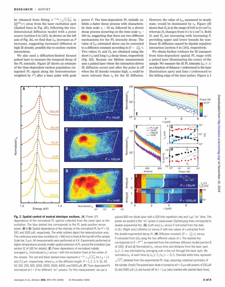
can bemanipulated by an in-plane electric field.Figure 3A shows the spatial map of IPL overlaidwith the device image when CIEs are opticallyexcited at the center of the sample. Similarto neutral IEs, CIEs generated at the laser-illuminated spot can diffuse across the entiresample. Both the WSe2 and MoSe2 layers inour device have multiple electrical contactsaway from the heterostructure edge (~10 mmaway) that are used to control the lateral elec-tric field while avoiding any local Schottkybarrier effects. Figure 3B shows the spatialmap of the PL intensity normalized as IPL(Vds)/IPL(Vds = 0) when applying an interlayer biasvoltage of Vds = 3 V across the WSe2 layer.We observe that the grounded edge of thesample becomes brighter with increasing Vds
(also see Fig. 3C for the normalized averageemission intensity along the heterostructurechannel). This increase in PL at the boundarybetween the heterostructure and the highlydopedmonolayer region can be explained bydrift of CIEs under the applied bias voltagein the channel. The applied bias Vds createsan electric field to tilt the band structure in thedirection of theWSe2 channel, driving positive(+) CIEs along the same direction as shownin the schematic diagram in Fig. 3D. At theboundary of the heterostructure, however, the+CIE cannot be transported to the WSe2 p-channel because current across the boundarymust be preserved. Therefore, the transported+CIEs recombine to turn into a hole in theWSe2p-channel. In figs. S13 and S14, we further con-firm this picture of CIE transport by changingthe doping polarity and Vds direction [see sec-tion 9 of (18) for details on gate configurationsand alternative explanations]. We also notethat, owing mainly to the limited resolutionof our electrical setup, we do not observe anyphotocurrent >10 pA.Finally, we demonstrate the electrical gen-
eration of IEs by free-carrier injection usingohmic contacts in individual TMD layers.Because our heterostructure forms type II–
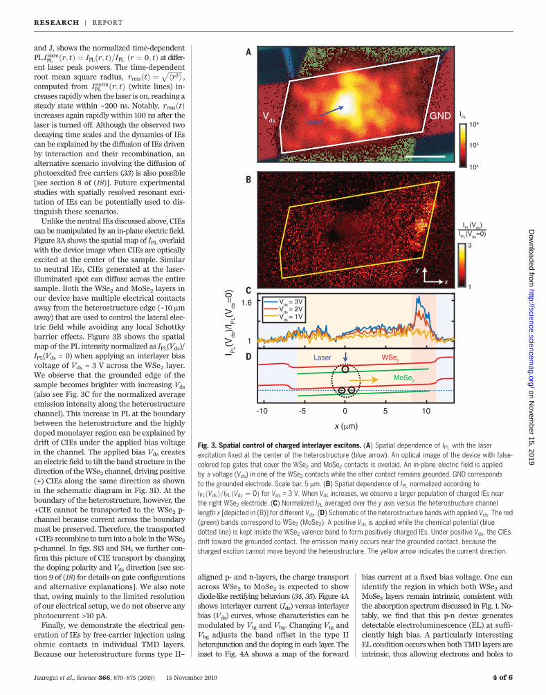
aligned p- and n-layers, the charge transportacross WSe2 to MoSe2 is expected to showdiode-like rectifying behaviors (34, 35). Figure 4Ashows interlayer current (Ids) versus interlayerbias (Vds) curves, whose characteristics can bemodulated by Vtg and Vbg. Changing Vtg andVbg adjusts the band offset in the type IIheterojunction and the doping in each layer. Theinset to Fig. 4A shows a map of the forward
bias current at a fixed bias voltage. One canidentify the region in which both WSe2 andMoSe2 layers remain intrinsic, consistent withthe absorption spectrum discussed in Fig. 1. No-tably, we find that this p-n device generatesdetectable electroluminescence (EL) at suffi-ciently high bias. A particularly interestingEL condition occurs when both TMD layers areintrinsic, thus allowing electrons and holes to
Jauregui et al., Science 366, 870–875 (2019) 15 November 2019 4 of 6
-
+ +
10
x (µm)
1
1.6
I PL(
Vds
)/I P
L(V
ds=
0)
0 5
Laser
Vds = 3VVds = 2VVds = 1V
WSe2
MoSe2
IPL(Vds)IPL(Vds=0)
3
1
A
B
C
D
-5-10
IPL
104
106LaserVds GND
x
y
105
Fig. 3. Spatial control of charged interlayer excitons. (A) Spatial dependence of IPL with the laserexcitation fixed at the center of the heterostructure (blue arrow). An optical image of the device with false-colored top gates that cover the WSe2 and MoSe2 contacts is overlaid. An in-plane electric field is appliedby a voltage (Vds) in one of the WSe2 contacts while the other contact remains grounded. GND correspondsto the grounded electrode. Scale bar, 5 mm. (B) Spatial dependence of IPL normalized according toIPLðVdsÞ=IPLðVds ¼ 0Þ for Vds = 3 V. When Vds increases, we observe a larger population of charged IEs nearthe right WSe2 electrode. (C) Normalized IPL averaged over the y axis versus the heterostructure channellength x [depicted in (B)] for different Vds. (D) Schematic of the heterostructure bands with applied Vds. The red(green) bands correspond to WSe2 (MoSe2). A positive Vds is applied while the chemical potential (bluedotted line) is kept inside the WSe2 valence band to form positively charged IEs. Under positive Vds, the CIEsdrift toward the grounded contact. The emission mainly occurs near the grounded contact, because thecharged exciton cannot move beyond the heterostructure. The yellow arrow indicates the current direction.
RESEARCH | REPORTon N
ovember 15, 2019
http://science.sciencem
ag.org/D
ownloaded from
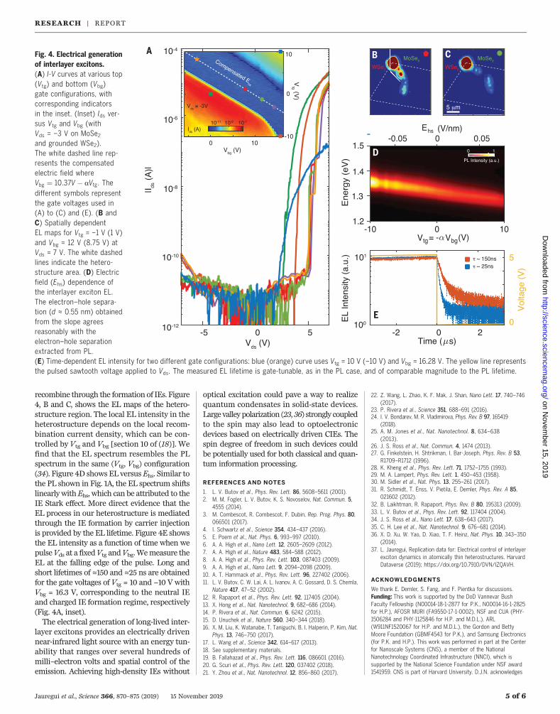
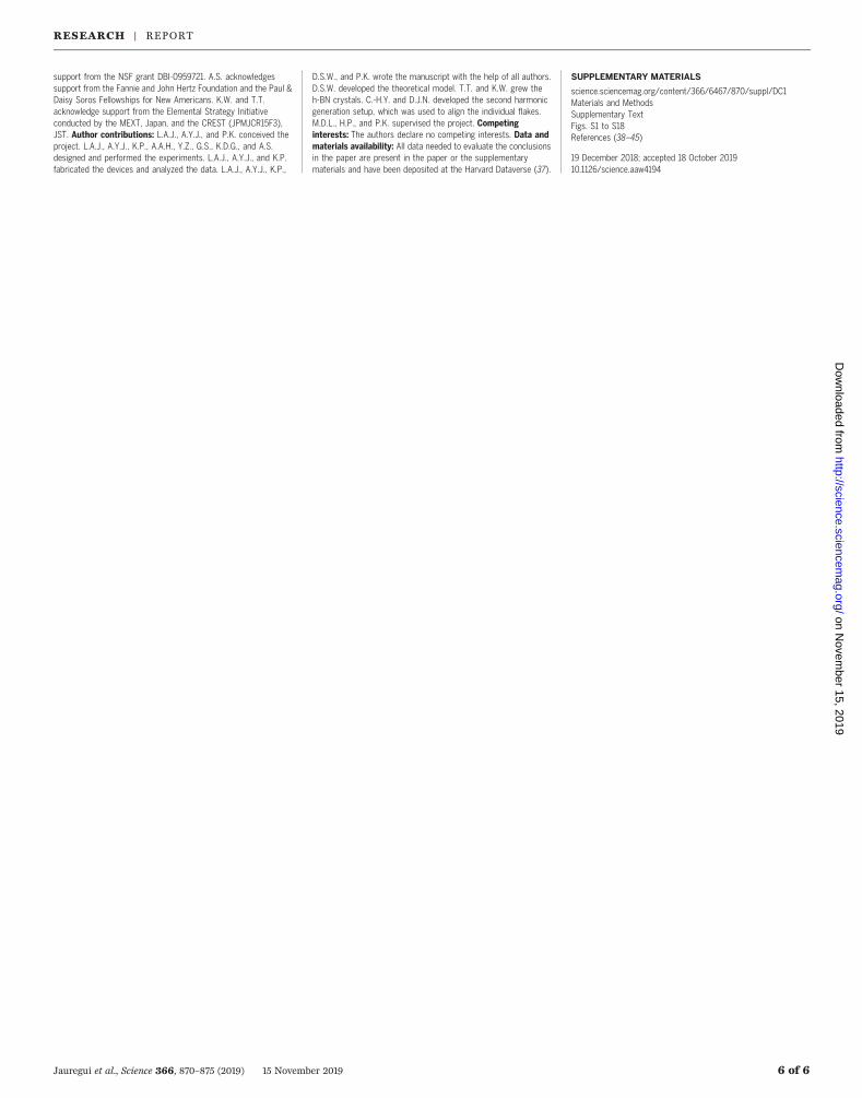
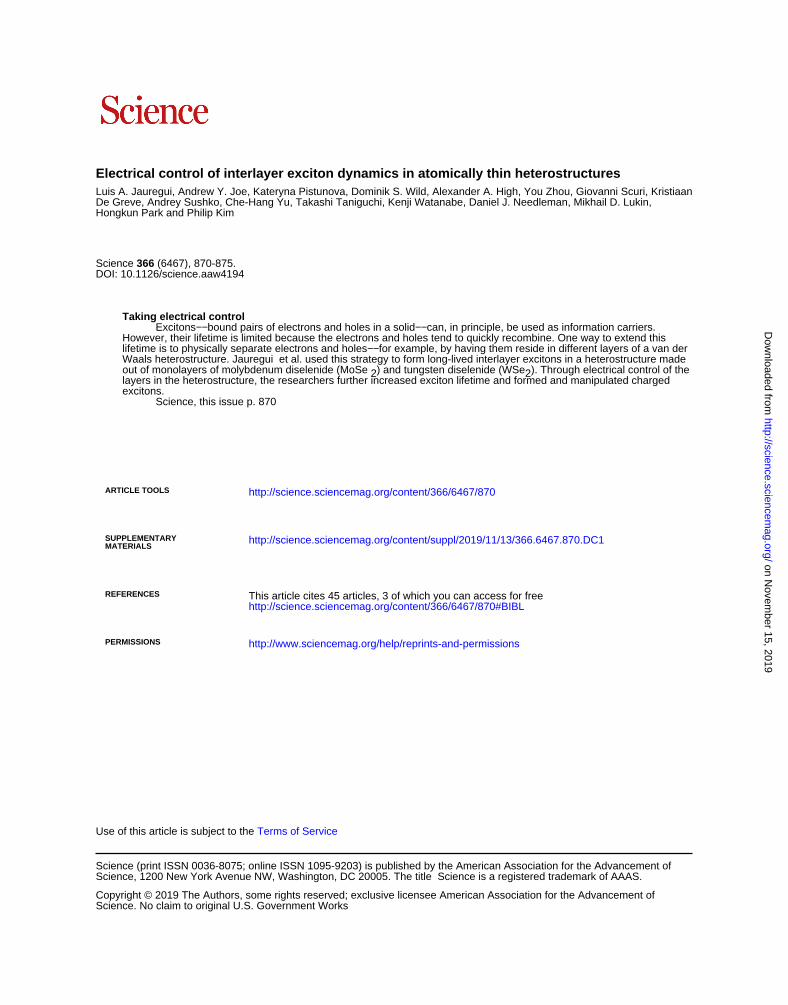
recombine through the formation of IEs. Figure4, B and C, shows the EL maps of the hetero-structure region. The local EL intensity in theheterostructure depends on the local recom-bination current density, which can be con-trolled by Vtg and Vbg [section 10 of (18)]. Wefind that the EL spectrum resembles the PLspectrum in the same (Vtg, Vbg) configuration(34). Figure 4D shows EL versus Ehs. Similar tothe PL shown in Fig. 1A, the EL spectrum shiftslinearly withEhs, which can be attributed to theIE Stark effect. More direct evidence that theEL process in our heterostructure is mediatedthrough the IE formation by carrier injectionis provided by the EL lifetime. Figure 4E showsthe EL intensity as a function of time when wepulseVds at a fixedVtg andVbg.Wemeasure theEL at the falling edge of the pulse. Long andshort lifetimes of ≈150 and ≈25 ns are obtainedfor the gate voltages of Vtg = 10 and −10 V withVbg = 16.3 V, corresponding to the neutral IEand charged IE formation regime, respectively(Fig. 4A, inset).The electrical generation of long-lived inter-
layer excitons provides an electrically drivennear-infrared light source with an energy tun-ability that ranges over several hundreds ofmilli–electron volts and spatial control of theemission. Achieving high-density IEs without
optical excitation could pave a way to realizequantum condensates in solid-state devices.Large valley polarization (23, 36) strongly coupledto the spin may also lead to optoelectronicdevices based on electrically driven CIEs. Thespin degree of freedom in such devices couldbe potentially used for both classical and quan-tum information processing.
REFERENCES AND NOTES
1. L. V. Butov et al., Phys. Rev. Lett. 86, 5608–5611 (2001).2. M. M. Fogler, L. V. Butov, K. S. Novoselov, Nat. Commun. 5,
4555 (2014).3. M. Combescot, R. Combescot, F. Dubin, Rep. Prog. Phys. 80,
066501 (2017).4. I. Schwartz et al., Science 354, 434–437 (2016).5. E. Poem et al., Nat. Phys. 6, 993–997 (2010).6. A. A. High et al., Nano Lett. 12, 2605–2609 (2012).7. A. A. High et al., Nature 483, 584–588 (2012).8. A. A. High et al., Phys. Rev. Lett. 103, 087403 (2009).9. A. A. High et al., Nano Lett. 9, 2094–2098 (2009).10. A. T. Hammack et al., Phys. Rev. Lett. 96, 227402 (2006).11. L. V. Butov, C. W. Lai, A. L. Ivanov, A. C. Gossard, D. S. Chemla,
Nature 417, 47–52 (2002).12. R. Rapaport et al., Phys. Rev. Lett. 92, 117405 (2004).13. X. Hong et al., Nat. Nanotechnol. 9, 682–686 (2014).14. P. Rivera et al., Nat. Commun. 6, 6242 (2015).15. D. Unuchek et al., Nature 560, 340–344 (2018).16. X. M. Liu, K. Watanabe, T. Taniguchi, B. I. Halperin, P. Kim, Nat.
Phys. 13, 746–750 (2017).17. L. Wang et al., Science 342, 614–617 (2013).18. See supplementary materials.19. B. Fallahazad et al., Phys. Rev. Lett. 116, 086601 (2016).20. G. Scuri et al., Phys. Rev. Lett. 120, 037402 (2018).21. Y. Zhou et al., Nat. Nanotechnol. 12, 856–860 (2017).
22. Z. Wang, L. Zhao, K. F. Mak, J. Shan, Nano Lett. 17, 740–746(2017).
23. P. Rivera et al., Science 351, 688–691 (2016).24. I. V. Bondarev, M. R. Vladimirova, Phys. Rev. B 97, 165419
(2018).25. A. M. Jones et al., Nat. Nanotechnol. 8, 634–638
(2013).26. J. S. Ross et al., Nat. Commun. 4, 1474 (2013).27. G. Finkelstein, H. Shtrikman, I. Bar-Joseph, Phys. Rev. B 53,
R1709–R1712 (1996).28. K. Kheng et al., Phys. Rev. Lett. 71, 1752–1755 (1993).29. M. A. Lampert, Phys. Rev. Lett. 1, 450–453 (1958).30. M. Sidler et al., Nat. Phys. 13, 255–261 (2017).31. R. Schmidt, T. Enss, V. Pietila, E. Demler, Phys. Rev. A 85,
021602 (2012).32. B. Laikhtman, R. Rapaport, Phys. Rev. B 80, 195313 (2009).33. L. V. Butov et al., Phys. Rev. Lett. 92, 117404 (2004).34. J. S. Ross et al., Nano Lett. 17, 638–643 (2017).35. C. H. Lee et al., Nat. Nanotechnol. 9, 676–681 (2014).36. X. D. Xu, W. Yao, D. Xiao, T. F. Heinz, Nat. Phys. 10, 343–350
(2014).37. L. Jauregui, Replication data for: Electrical control of interlayer
exciton dynamics in atomically thin heterostructures. HarvardDataverse (2019); https://doi.org/10.7910/DVN/IZQAVH.
ACKNOWLEDGMENTS
We thank E. Demler, S. Fang, and F. Pientka for discussions.Funding: This work is supported by the DoD Vannevar BushFaculty Fellowship (N00014-18-1-2877 for P.K., N00014-16-1-2825for H.P.), AFOSR MURI (FA9550-17-1-0002), NSF and CUA (PHY-1506284 and PHY-1125846 for H.P. and M.D.L.), ARL(W911NF1520067 for H.P. and M.D.L.), the Gordon and BettyMoore Foundation (GBMF4543 for P.K.), and Samsung Electronics(for P.K. and H.P.). This work was performed in part at the Centerfor Nanoscale Systems (CNS), a member of the NationalNanotechnology Coordinated Infrastructure (NNCI), which issupported by the National Science Foundation under NSF award1541959. CNS is part of Harvard University. D.J.N. acknowledges
Jauregui et al., Science 366, 870–875 (2019) 15 November 2019 5 of 6
Fig. 4. Electrical generationof interlayer excitons.(A) I-V curves at various top(Vtg) and bottom (Vbg)gate configurations, withcorresponding indicatorsin the inset. (Inset) Ids ver-sus Vtg and Vbg (withVds = −3 V on MoSe2and grounded WSe2).The white dashed line rep-resents the compensatedelectric field whereVbg ¼ 10:37V � aVtg. Thedifferent symbols representthe gate voltages used in(A) to (C) and (E). (B andC) Spatially dependentEL maps for Vtg = −1 V (1 V)and Vbg = 12 V (8.75 V) atVds = 7 V. The white dashedlines indicate the hetero-structure area. (D) Electricfield (Ehs) dependence ofthe interlayer exciton EL.The electron–hole separa-tion (d ≈ 0.55 nm) obtainedfrom the slope agreesreasonably with theelectron–hole separationextracted from PL.(E) Time-dependent EL intensity for two different gate configurations: blue (orange) curve uses Vtg = 10 V (−10 V) and Vbg = 16.28 V. The yellow line representsthe pulsed sawtooth voltage applied to Vds. The measured EL lifetime is gate-tunable, as in the PL case, and of comparable magnitude to the PL lifetime.
RESEARCH | REPORTon N
ovember 15, 2019
http://science.sciencem
ag.org/D
ownloaded from
support from the NSF grant DBI-0959721. A.S. acknowledgessupport from the Fannie and John Hertz Foundation and the Paul &Daisy Soros Fellowships for New Americans. K.W. and T.T.acknowledge support from the Elemental Strategy Initiativeconducted by the MEXT, Japan, and the CREST (JPMJCR15F3),JST. Author contributions: L.A.J., A.Y.J., and P.K. conceived theproject. L.A.J., A.Y.J., K.P., A.A.H., Y.Z., G.S., K.D.G., and A.S.designed and performed the experiments. L.A.J., A.Y.J., and K.P.fabricated the devices and analyzed the data. L.A.J., A.Y.J., K.P.,
D.S.W., and P.K. wrote the manuscript with the help of all authors.D.S.W. developed the theoretical model. T.T. and K.W. grew theh-BN crystals. C.-H.Y. and D.J.N. developed the second harmonicgeneration setup, which was used to align the individual flakes.M.D.L., H.P., and P.K. supervised the project. Competinginterests: The authors declare no competing interests. Data andmaterials availability: All data needed to evaluate the conclusionsin the paper are present in the paper or the supplementarymaterials and have been deposited at the Harvard Dataverse (37).
SUPPLEMENTARY MATERIALS
science.sciencemag.org/content/366/6467/870/suppl/DC1Materials and MethodsSupplementary TextFigs. S1 to S18References (38–45)
19 December 2018; accepted 18 October 201910.1126/science.aaw4194
Jauregui et al., Science 366, 870–875 (2019) 15 November 2019 6 of 6
RESEARCH | REPORTon N
ovember 15, 2019
http://science.sciencem
ag.org/D
ownloaded from
Electrical control of interlayer exciton dynamics in atomically thin heterostructures
Hongkun Park and Philip KimDe Greve, Andrey Sushko, Che-Hang Yu, Takashi Taniguchi, Kenji Watanabe, Daniel J. Needleman, Mikhail D. Lukin, Luis A. Jauregui, Andrew Y. Joe, Kateryna Pistunova, Dominik S. Wild, Alexander A. High, You Zhou, Giovanni Scuri, Kristiaan
DOI: 10.1126/science.aaw4194 (6467), 870-875.366Science
, this issue p. 870Scienceexcitons.layers in the heterostructure, the researchers further increased exciton lifetime and formed and manipulated charged
). Through electrical control of the2) and tungsten diselenide (WSe2out of monolayers of molybdenum diselenide (MoSe used this strategy to form long-lived interlayer excitons in a heterostructure madeet al.Waals heterostructure. Jauregui
for example, by having them reside in different layers of a van der−−lifetime is to physically separate electrons and holes However, their lifetime is limited because the electrons and holes tend to quickly recombine. One way to extend this
can, in principle, be used as information carriers.−−bound pairs of electrons and holes in a solid−−ExcitonsTaking electrical control
ARTICLE TOOLS http://science.sciencemag.org/content/366/6467/870
MATERIALSSUPPLEMENTARY http://science.sciencemag.org/content/suppl/2019/11/13/366.6467.870.DC1
REFERENCES
http://science.sciencemag.org/content/366/6467/870#BIBLThis article cites 45 articles, 3 of which you can access for free
PERMISSIONS http://www.sciencemag.org/help/reprints-and-permissions
Terms of ServiceUse of this article is subject to the
is a registered trademark of AAAS.ScienceScience, 1200 New York Avenue NW, Washington, DC 20005. The title (print ISSN 0036-8075; online ISSN 1095-9203) is published by the American Association for the Advancement ofScience
Science. No claim to original U.S. Government WorksCopyright © 2019 The Authors, some rights reserved; exclusive licensee American Association for the Advancement of
on Novem
ber 15, 2019
http://science.sciencemag.org/
Dow
nloaded from