1-electrónica analógica de comunicaciones
DESCRIPTION
Curso de electrónica analógica de comunicacionesTRANSCRIPT

Electrónica Analógica de Comunicaciones.
GRUPO: 8CV03SEPTIEMBRE-DICIMEBRE 2015
LABORATORIO: MARTES 16:00-17:30TEORÍA: MIÉRCOLES 19:00-20:30 SALON 5106
TEORÍA JUEVES: 20:30-22:00 SALON 5112ROBERTO LINARES Y MIRANDA

PRIMERA PARTE• Procesos de fabricación de circuitos integrados de alta y baja frecuencia. • Parámetros de dispersión. • Filtros pasivos Butterworth y Chebyshev. • Filtro pasa bajas. • Filtro pasa altas. • Filtro pasa banda. • Filtro elimina banda. • Simulación asistida por computadora para el diseño de • filtros pasivos S Pice. • Filtros activos Butterworth y Chebyshev. • Filtro pasa baja. • Filtro pasa altas. • Filtro pasa banda. • Filtro elimina banda • Simulación asistida por computadora para el diseño de • filtros activos S Pice. • Comparación entre filtros pasivos y activos. • Distorsión lineal. •
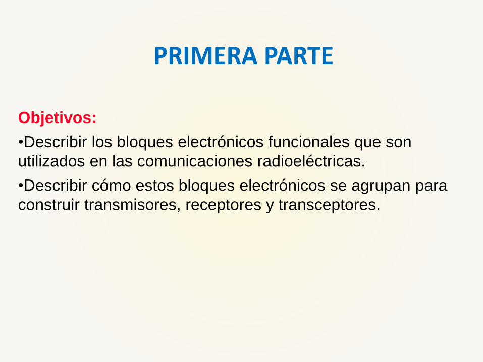
Objetivos:
•Describir los bloques electrónicos funcionales que son
utilizados en las comunicaciones radioeléctricas.
•Describir cómo estos bloques electrónicos se agrupan para
construir transmisores, receptores y transceptores.
PRIMERA PARTE

1. Introducción a la Electrónica de
Comunicaciones
Información
Transmisor
Información
ReceptorMedio
físico
Transmisión de la
información a distancia

Información
Transmisor
Información
Receptor
Transmisión radioeléctrica de la información (I)
Línea de
transmisión
Antena
Línea de
transmisión
Antena

Transmisión radioeléctrica de la información (II)
Información
Transmisor
Información
Receptor
Línea de
transmisión
Antena
Línea de
transmisión
Antena
• Dispositivos Electrónicos
• Electrónica Analógica
• Electrónica Digital
• Sistemas Electrónicos Digitales
• Campos
Electromagnéticos (I y II)
• Radiación y
Radiopropagación
Electrónica de
Comunicaciones
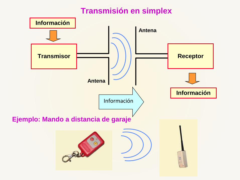
Transmisión en simplex
Información
Transmisor
Antena
Información
Receptor
Antena
Ejemplo: Mando a distancia de garaje
Información

Transmisión en semiduplex (half duplex), (I)
Información Antena
Transmisor
Receptor
Conmutador
InformaciónAntena
Transmisor
Receptor
Conmutador
Información
Información Antena
Transmisor
Receptor
Conmutador
InformaciónAntena
Transmisor
Receptor
Conmutador
Información

Transmisión en semiduplex (half duplex), (I)
Información Antena
Transmisor
Receptor
Conmutador
InformaciónAntena
Transmisor
Receptor
Conmutador
Información
Información Antena
Transmisor
Receptor
Conmutador
InformaciónAntena
Transmisor
Receptor
Conmutador
Información
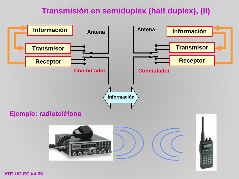
Transmisión en semiduplex (half duplex), (II)
Ejemplo: radioteléfono
Información Antena InformaciónAntena
Transmisor
Receptor
Transmisor
Receptor
Conmutador Conmutador
Información
ATE-UO EC int 06
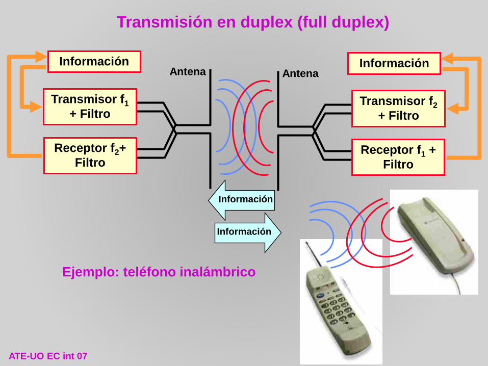
Transmisión en duplex (full duplex)
Ejemplo: teléfono inalámbrico
InformaciónAntena
Transmisor f1
+ Filtro
Receptor f2+
Filtro
InformaciónAntena
Transmisor f2
+ Filtro
Receptor f1 +
Filtro
Información
Información
ATE-UO EC int 07

Ejemplo de receptor: Receptor Superheterodino
Filtro
de RF
Antena
Información
Amplificador
de RF
Mezclador
Filtro
de FI
Amplificador
de FI
Oscilador Local
Demodulador
Amplificador
de BB
RF: Radio Frecuencia
FI: Frecuencia Intermedia
BB: Banda Base
Bloques electrónicos funcionales:
Oscilador.
Mezclador.
Amplificadores de pequeña señal.
Filtros pasa-banda.
Demodulador.
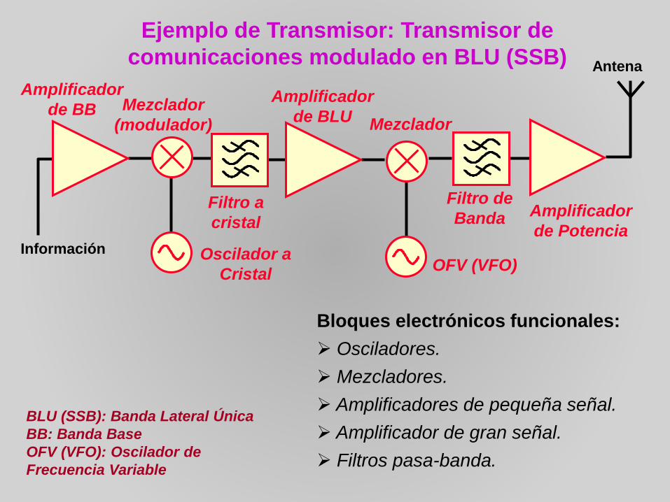
Ejemplo de Transmisor: Transmisor de
comunicaciones modulado en BLU (SSB)
Filtro a
cristalAmplificador
de Potencia
Mezclador
(modulador)
Filtro de
Banda
Amplificador
de BLU
Oscilador a
Cristal
Amplificador
de BB
BLU (SSB): Banda Lateral Única
BB: Banda Base
OFV (VFO): Oscilador de
Frecuencia Variable
Bloques electrónicos funcionales:
Osciladores.
Mezcladores.
Amplificadores de pequeña señal.
Amplificador de gran señal.
Filtros pasa-banda.
Información
Antena
OFV (VFO)
Mezclador


S-P
ara
mete
rsEE 5
64
Transmission Lines2 Port Networks & S-Parameters
38
S-P
ara
mete
rsEE 5
64
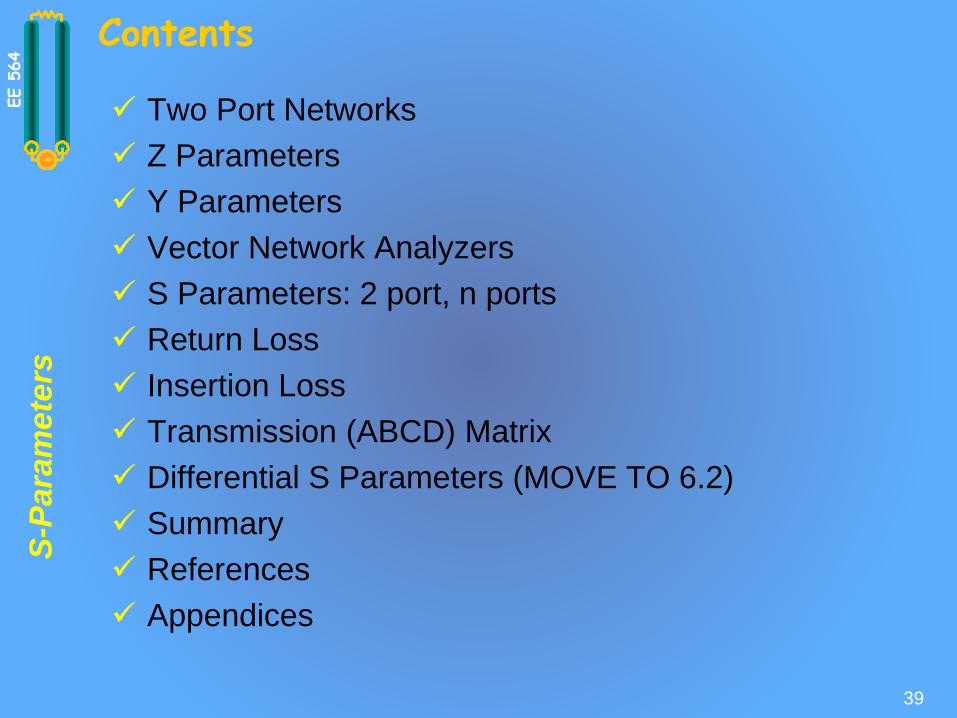
Contents
Two Port Networks
Z Parameters
Y Parameters
Vector Network Analyzers
S Parameters: 2 port, n ports
Return Loss
Insertion Loss
Transmission (ABCD) Matrix
Differential S Parameters (MOVE TO 6.2)
Summary
References
Appendices
39

S-P
ara
mete
rsEE 5
64
Two Port Networks Linear networks can be completely characterized by
parameters measured at the network ports without knowing the content of the networks.
Networks can have any number of ports. Analysis of a 2-port network is sufficient to explain the theory
and applies to isolated signals (no crosstalk).
The ports can be characterized with many parameters (Z, Y, S, ABDC). Each has a specific advantage.
Each parameter set is related to 4 variables: 2 independent variables for excitation
2 dependent variables for response
40
2 Port
NetworkPo
rt 1
I1
+
-
V1
Po
rt 2I
2
+
-
V2
S-P
ara
mete
rsEE 5
64
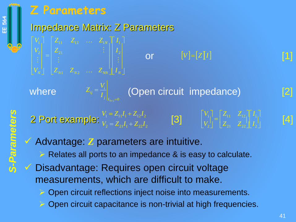
Z Parameters
Advantage: Z parameters are intuitive.
Relates all ports to an impedance & is easy to calculate.
Disadvantage: Requires open circuit voltage
measurements, which are difficult to make.
Open circuit reflections inject noise into measurements.
Open circuit capacitance is non-trivial at high frequencies.
41
NNNNN
N
N I
I
I
ZZZ
Z
ZZZ
V
V
V
2
1
21
21
11211
2
1
IZV
0
jkIj
iij
I
VZ (Open circuit impedance)
Impedance Matrix: Z Parameters
or [1]
where [2]
2221212
2121111
IZIZV
IZIZV
2 Port example:
2
1
2221
1211
2
1
I
I
ZZ
ZZ
V
V[4][3]

S-P
ara
mete
rsEE 5
64
Y Parameters
42
NNNNN
N
N V
V
V
YYY
Y
YYY
I
I
I
2
1
21
21
11211
2
1
VYI
0
jkVj
iij
V
IY (Short circuit admittance)
Admittance Matrix: Y Parameters
or
[6]
[5]
where
2221212
2121111
VYVYI
VYVYI
2 Port example:
2
1
2221
1211
2
1
V
V
YY
YY
I
I
Advantage: Y parameters are also somewhat intuitive.
Disadvantage: Requires short circuit voltage
measurements, which are difficult to make.
Short circuit reflections inject noise into measurements.
Short circuit inductance is non-trivial at high frequencies.
[7] [8]

S-P
ara
mete
rsEE 5
64
Example
43
ZC
ZA
ZB
+
-
+
-
V1
V2
I1
I2
Po
rt 1
Po
rt 2
CA
CA
I
ZZ
ZZV
V
I
VZ
1
1
1
111
02
CC
I
ZI
ZI
I
VZ
2
2
2
112
01
CC
I
ZI
ZI
I
VZ
1
1
1
221
02
CB
CB
I
ZZ
ZZV
V
I
VZ
2
2
2
222
01

S-P
ara
mete
rsEE 5
64
Frequency Domain: Vector Network Analyzer (VNA)
VNA offers a means to
characterize circuit elements
as a function of frequency.
44
VNA is a microwave based instrument that provides the
ability to understand frequency dependent effects.
The input signal is a frequency swept sinusoid.
Characterizes the network by observing transmitted and
reflected power waves.
Voltage and current are difficult to measure directly.
It is also difficult to implement open & short circuit loads at high
frequency.
Matched load is a unique, repeatable termination, and is
insensitive to length, making measurement easier.
Incident and reflected waves the key measures.
We characterize the device under test using S parameters.
2-Port
NetworkV
1
+
V2
I1
I2
-
+
-

S-P
ara
mete
rsEE 5
64
S Parameters
We wish to characterize the network by observing
transmitted and reflected power waves.
ai represents the square root of the power wave injected into port i.
bi represents the square root of the power wave injected into port j.
45
2 Port
Network
a1
+
-
V1
Po
rt 2
a2
+
-
V2
Po
rt 1
b1
b2
RVP
2
R
VPai
1
R
Vb
j
j
use
to get
[9]
[10]
[11]
S-P
ara
mete
rsEE 5
64
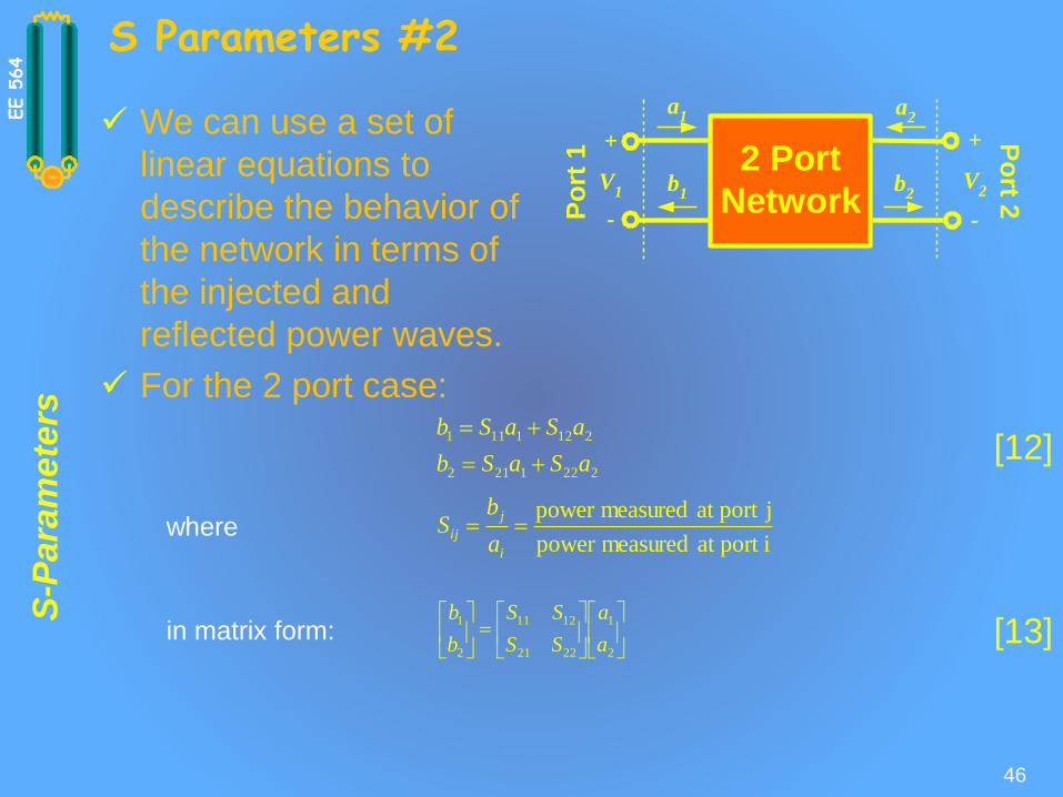
S Parameters #2
We can use a set of
linear equations to
describe the behavior of
the network in terms of
the injected and
reflected power waves.
For the 2 port case:
2
1
2221
1211
2
1
a
a
SS
SS
b
b
46
2 Port
Network
a1
+
-
V1
Po
rt 2
a2
+
-
V2
Po
rt 1
b1
b2
2221212
2121111
aSaSb
aSaSb
iport at measuredpower
jport at measuredpower
i
j
ija
bSwhere
in matrix form:
[12]
[13]

S-P
ara
mete
rsEE 5
64
S Parameters – n Ports
47
[5.5.14]
[17]
n
nn
Z
Va
0
aSb
n
nn
Z
Vb
0
jkk
jkk
Vj
j
i
i
aj
iij
Z
V
Z
V
a
bS
,0
,0
0
0
nnnn
N
n a
a
a
SS
S
SSS
b
b
b
2
1
1
21
11211
2
1
nnnnnn
nn
nn
aSaSaSb
aSaSaSb
aSaSaSb
2211
22221212
12121111
or
[15]
[16]
[18]
S-P
ara
mete
rsEE 5
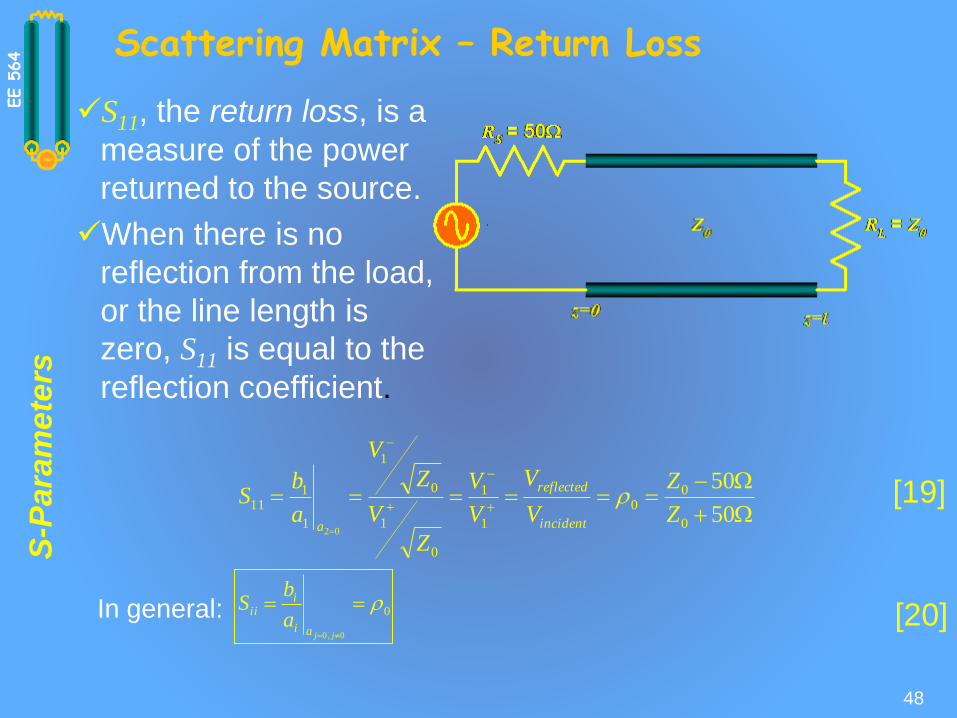
64 Scattering Matrix – Return Loss
S11, the return loss, is a
measure of the power
returned to the source.
When there is no
reflection from the load,
or the line length is
zero, S11 is equal to the
reflection coefficient.
48
50
50
0
00
1
1
0
1
0
1
1
111
02
Z
Z
V
V
V
V
Z
V
Z
V
a
bS
incident
reflected
a
[19]
0
0,0
jjai
iii
a
bSIn general: [20]
S-P
ara
mete
rsEE 5
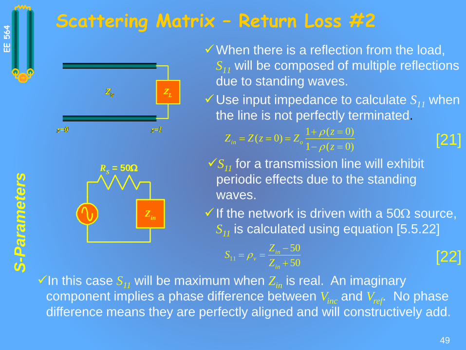
64 Scattering Matrix – Return Loss #2
When there is a reflection from the load,
S11 will be composed of multiple reflections
due to standing waves.
Use input impedance to calculate S11 when
the line is not perfectly terminated.
49
)0(1
)0(1)0(
z
zZzZZ oin
If the network is driven with a 50 source,
S11 is calculated using equation [5.5.22]
RS = 50
Zin
S11 for a transmission line will exhibit
periodic effects due to the standing
waves.
In this case S11 will be maximum when Zin is real. An imaginary
component implies a phase difference between Vinc and Vref. No phase
difference means they are perfectly aligned and will constructively add.
50
5011
in
inv
Z
ZS
[21]
[22]
S-P
ara
mete
rsEE 5
64
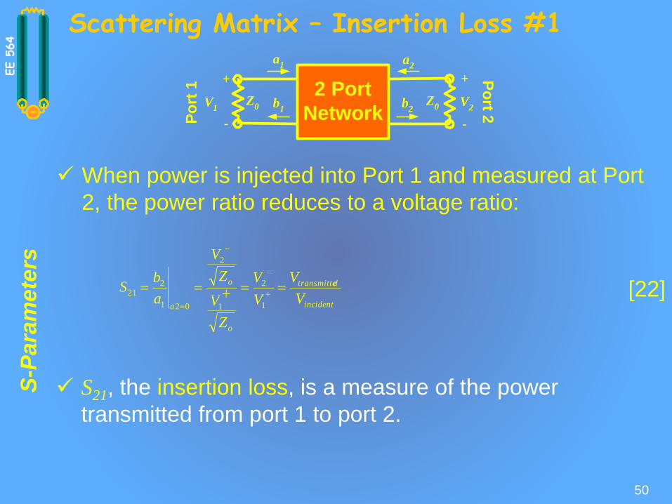
Scattering Matrix – Insertion Loss #1
When power is injected into Port 1 and measured at Port
2, the power ratio reduces to a voltage ratio:
50
incident
dtransmitte
o
o
aV
V
V
V
Z
V
Z
V
a
bS
1
2
1
2
021
221
2 Port
Network
a1
+
-
V1
Po
rt 2
a2
+
-
V2
Po
rt 1
b1
b2
Z0
Z0
S21, the insertion loss, is a measure of the power
transmitted from port 1 to port 2.
[22]

S-P
ara
mete
rsEE 5
64
Comments On “Loss”
True losses come from physical energy losses.
Ohmic (i.e. skin effect)
Field dampening effects (loss tangent)
Radiation (EMI)
Insertion and return losses include other effects, such
as impedance discontinuities and resonance, which
are not true losses.
Loss free networks can still exhibit significant insertion
and return losses due to impedance discontinuities.
51

S-P
ara
mete
rsEE 5
64
Reflection Coefficients
Reflection coefficient at the load:
52
0
0
ZZ
ZZ
L
LL
0
0
ZZ
ZZ
S
SS
L
L
L
Lin
S
SS
S
SSS
11
2
1211
22
211211
11
S
Sout
S
SSS
11
211222
1
[23]
[24]
[25]
[26]
Reflection coefficient at the source:
Input reflection coefficient:
Output reflection coefficient:
Assuming S12 = S21 and S11 = S22.
S-P
ara
mete
rsEE 5
64
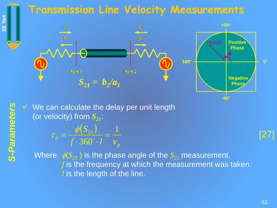
Transmission Line Velocity Measurements
53
We can calculate the delay per unit length
(or velocity) from S21:
S21 = b2/a1
p
dvlf
S 1
360
21
Where (S21 ) is the phase angle of the S21 measurement.
f is the frequency at which the measurement was taken.
l is the length of the line.
[27]
0°180°
+90°
-90°
Positive
Phase
Negative
Phase
0.8 135°

S-P
ara
mete
rsEE 5
64
Transmission Line Z0 Measurements
Impedance vs. frequency
Recall
Zin vs f will be a function of delay () and ZL.
We can use Zin equations for open and short circuited
lossy transmission.
54
lZZ openin tanh0,
lZZ shortin coth0,
lj
lj
ine
eZZ
2
2
01
1
openinshortin ZZZ ,,0
[28]
[29]
[30]
Using the equation for Zin,
in, and Z0, we can find the
impedance.

S-P
ara
mete
rsEE 5
64
Transmission Line Z0 Measurement #2
Input reflection coefficients for the open and short circuit cases:
55
shortin
shortin
VNAj
shortin
j
shortin
VNAshortin Ze
eZZ
,
,
02
,
02
,
,1
1
1
1
openinshortin ZZZ ,,0
[31]
[32]
11
2
1211
11
2
1211,
111
1
S
SS
S
SSopenin
11
2
1211
11
2
1211,
111
1
S
SS
S
SSshortin
openin
openin
VNAj
openin
j
openin
VNAopenin Ze
eZZ
,
,
02
,
02
,
,1
1
1
1
Input impedance for the open and short circuit cases:
Now we can apply equation [5.5.30]:
S-P
ara
mete
rsEE 5
64
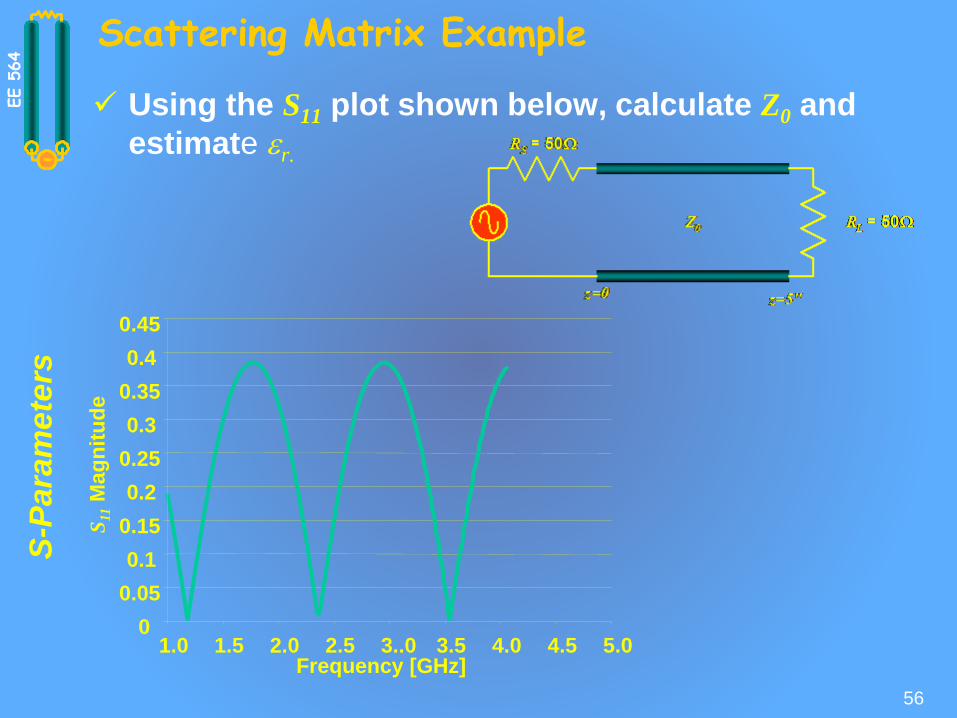
Scattering Matrix Example
Using the S11 plot shown below, calculate Z0 and
estimate er.
56
01.0 1.5 2.0 2.5 3..0 3.5 4.0 4.5 5.0
Frequency [GHz]
0.05
0.1
0.15
0.2
0.25
0.3
0.35
0.4
0.45
S11
Mag
nit
ud
e
S-P
ara
mete
rsEE 5
64
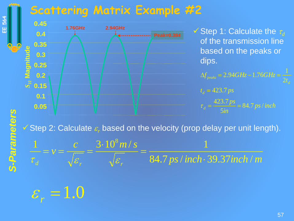
Scattering Matrix Example #2
57
1.76GHz 2.94GHzStep 1: Calculate the d
of the transmission line
based on the peaks or
dips.
d
peakst
GHzGHzf2
176.194.2
Step 2: Calculate er based on the velocity (prop delay per unit length).
minchinchps
smcv
rrd /37.39/7.84
1/1031 8
ee
Peak=0.384
0.05
0.1
0.15
0.2
0.25
0.3
0.35
0.4
0.45S
11
Mag
nit
ud
e
0.1re
pstd 7.423
inchpsin
psd /7.84
5
7.423
S-P
ara
mete
rsEE 5
64
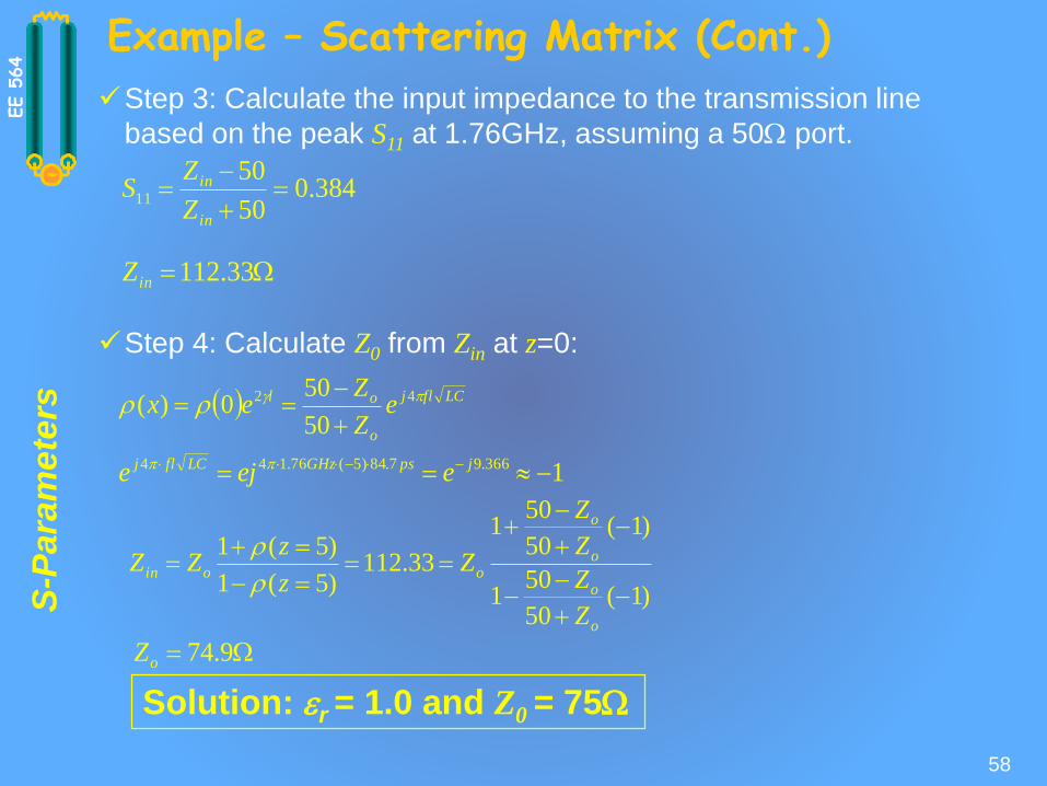
Example – Scattering Matrix (Cont.)
58
Step 3: Calculate the input impedance to the transmission line
based on the peak S11 at 1.76GHz, assuming a 50 port.
384.050
5011
in
in
Z
ZS
Step 4: Calculate Z0 from Zin at z=0:
LCflj
o
ol eZ
Zex 42
50
500)(
Solution: er = 1.0 and Z0 = 75
33.112inZ
1366.97.84)5(76.144 jpsGHzLCflj eeje
)1(50
501
)1(50
501
33.112)5(1
)5(1
o
o
o
o
ooin
Z
Z
Z
Z
Zz
zZZ
9.74oZ

S-P
ara
mete
rsEE 5
64 Advantages/Disadvantages of S Parameters
Advantages:
Ease of measurement: It is much easier to measure
power at high frequencies than open/short current and
voltage.
Disadvantages:
They are more difficult to understand and it is more
difficult to interpret measurements.
59

Transmission line equivalent
circuits and relevant
equations
Physics of transmission line structures
Basic transmission line equivalent circuit
?Equations for transmission line propagation

E & H Fields – Microstrip Case
The signal is really the wave propagating between the conductors
Remember fields are setup given
an applied forcing function.
(Source)
How does the signal move
from source to load?
Electric field
Magnetic field
Ground return path
X
Y
Z (into the page)
Signal path
Electric field
Magnetic field
Ground return path
X
Y
Z (into the page)
Signal path

Transmission Line “Definition”
• General transmission line: a closed system in which power is transmitted from a source to a destination
• Our class: only TEM mode transmission lines– A two conductor wire system with the wires in close proximity, providing
relative impedance, velocity and closed current return path to the source.– Characteristic impedance is the ratio of the voltage and current waves at
any one position on the transmission line
– Propagation velocity is the speed with which signals are transmitted through the transmission line in its surrounding medium.
I
VZ 0
r
cv
e

Presence of Electric and Magnetic Fields
• Both Electric and Magnetic fields are present in the transmission lines– These fields are perpendicular to each other and to the direction of wave
propagation for TEM mode waves, which is the simplest mode, and assumed for most simulators(except for microstrip lines which assume “quasi-TEM”, which is an approximated equivalent for transient response calculations).
• Electric field is established by a potential difference between two conductors.
– Implies equivalent circuit model must contain capacitor.
• Magnetic field induced by current flowing on the line– Implies equivalent circuit model must contain inductor.
V
I
I
E
+
-
+
-
+
-
+
-
V + V
I + I
I + I
V
IH
IH
V + V
I + I
I + I
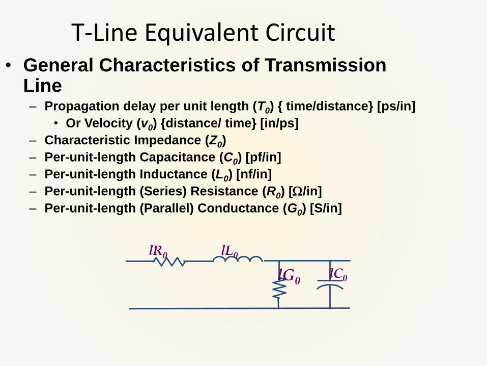
• General Characteristics of Transmission Line– Propagation delay per unit length (T0) { time/distance} [ps/in]
• Or Velocity (v0) {distance/ time} [in/ps]
– Characteristic Impedance (Z0)
– Per-unit-length Capacitance (C0) [pf/in]
– Per-unit-length Inductance (L0) [nf/in]
– Per-unit-length (Series) Resistance (R0) [/in]
– Per-unit-length (Parallel) Conductance (G0) [S/in]
T-Line Equivalent Circuit
lL0lR0
lC0lG0

Ideal T Line
• Ideal (lossless) Characteristics of Transmission Line– Ideal TL assumes:
• Uniform line
• Perfect (lossless) conductor (R00)
• Perfect (lossless) dielectric (G00)
– We only consider T0, Z0 , C0, and L0.
• A transmission line can be represented by a cascaded network (subsections) of these equivalent models. – The smaller the subsection the more accurate the model
– The delay for each subsection should be no larger than 1/10th the signal rise time.
lL0
lC0
Signal Frequency and Edge Rate vs.
Lumped or Tline Models
In theory, all circuits that deliver transient power from
one point to another are transmission lines, but if the
signal frequency(s) is low compared to the size of the
circuit (small), a reasonable approximation can be
used to simplify the circuit for calculation of the circuit
transient (time vs. voltage or time vs. current)
response.

T Line Rules of Thumb
Td < .1 Tx
Td < .4 Tx
May treat as lumped Capacitance Use this 10:1 ratio for accurate modeling of transmission lines
May treat as RC on-chip, and treat as LC for PC board interconnect
So, what are the rules of thumb to use?
Other “Rules of Thumb”
• Frequency knee (Fknee) = 0.35/Tr (so if Tr is 1nS, Fknee is 350MHz)
• This is the frequency at which most energy is below
• Tr is the 10-90% edge rate of the signal
• Assignment: At what frequency can your thumb be used to determine which elements are lumped?– Assume 150 ps/in
Equations & Formulas
• How to model & explain transmission line behavior
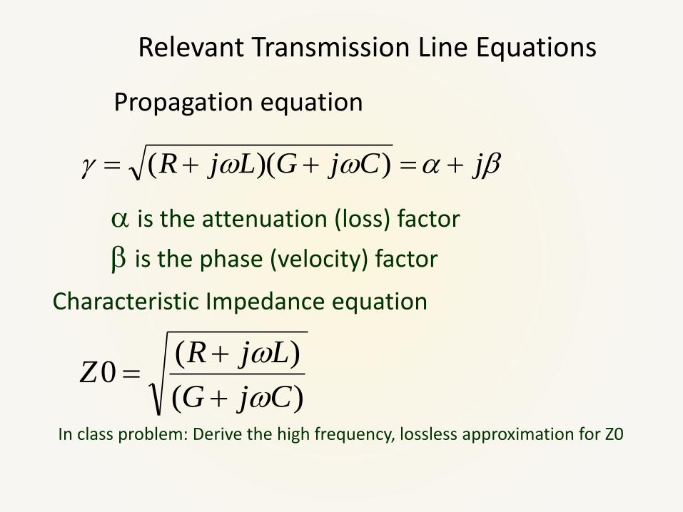
Relevant Transmission Line Equations
Propagation equation
jCjGLjR ))((
)(
)(0
CjG
LjRZ
Characteristic Impedance equation
In class problem: Derive the high frequency, lossless approximation for Z0
is the attenuation (loss) factor
is the phase (velocity) factor
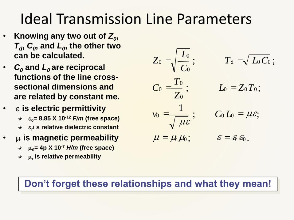
Ideal Transmission Line Parameters• Knowing any two out of Z0,
Td, C0, and L0, the other two
can be calculated.
• C0 and L0 are reciprocal
functions of the line cross-
sectional dimensions and
are related by constant me.
• e is electric permittivitye0= 8.85 X 10⁻¹² F/m (free space)
eri s relative dielectric constant
• m is magnetic permeabilitym0= 4p X 10-7 H/m (free space)
mr is relative permeability
.;
;;1
;;
;;
00
000
000
0
00
00d
0
00
eeemmm
meme
rr
LCv
TZLZ
TC
CLTC
LZ
Don’t forget these relationships and what they mean!
Parallel Plate Approximation
• Assumptions– TEM conditions
– Uniform dielectric (e ) between conductors
– TC<< TD; WC>> TD• T-line characteristics are
function of:– Material electric and magnetic
properties– Dielectric Thickness (TD)– Width of conductor (WC)
• Trade-off– TD ; C0 , L0 , Z0
– WC ; C0 , L0 , Z0
TD
TC
WC
e
To a first order, t-line capacitance and inductance can
be approximated using the parallel plate approximation.
d
PlateAreaC
*e Base
equation
C0 eWC
TD
F
m
8.85 e rWC
TD
pF
m
L0 mTD
WC
F
m
0.4 mrTD
WC
mH
m
Z0 377TD
WC
mr
e r
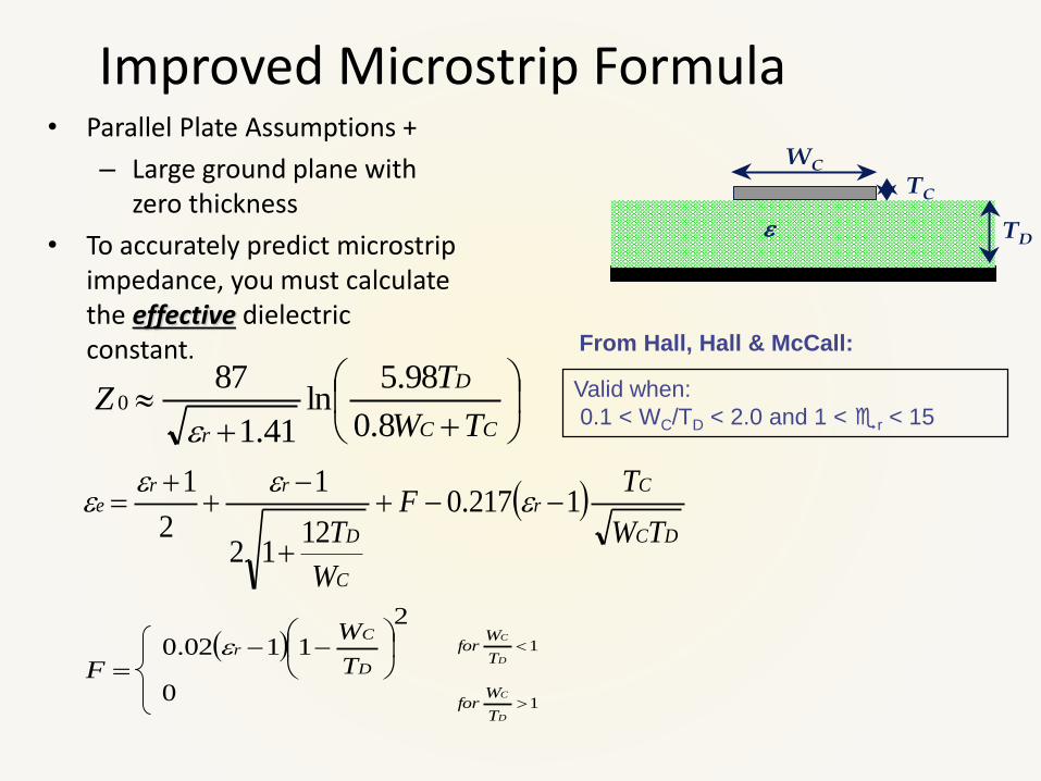
Improved Microstrip Formula• Parallel Plate Assumptions +
– Large ground plane with zero thickness
• To accurately predict microstripimpedance, you must calculate the effective dielectric constant.
TD
TC
e
WC
From Hall, Hall & McCall:
CC
D
r TW
TZ
8.0
98.5ln
41.1
870
e
DC
Cr
C
D
rre
TW
TF
W
T1217.0
1212
1
2
1
e
eee
2
1102.0
D
Cr
T
We
F1
D
C
T
Wfor
01
D
C
T
Wfor
Valid when:
0.1 < WC/TD < 2.0 and 1 < er < 15
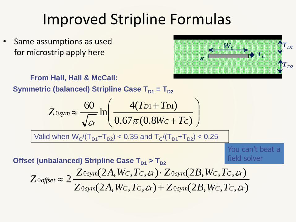
Improved Stripline Formulas• Same assumptions as used
for microstrip apply here
TD2
TCe
WCTD1
From Hall, Hall & McCall:
)8.0(67.0
)(4ln
60 110
CC
DD
r
sym
TW
TTZ
e
Symmetric (balanced) Stripline Case TD1 = TD2
),,,2(),,,2(
),,,2(),,,2(2
00
000
rCCsymrCCsym
rCCsymrCCsymoffset
TWBZTWAZ
TWBZTWAZZ
ee
ee
Offset (unbalanced) Stripline Case TD1 > TD2
Valid when WC/(TD1+TD2) < 0.35 and TC/(TD1+TD2) < 0.25
You can’t beat a field solver

Special Cases to Remember
1
Zo
Zo
0
ZoZo
ZoZo
10
0
Zo
Zo
Vs
ZsZo Zo
A: Terminated in Zo
Vs
ZsZo
B: Short Circuit
Vs
ZsZo
C: Open Circuit
S-P
ara
mete
rsEE 5
64
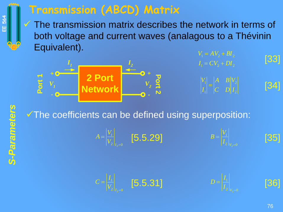
Transmission (ABCD) Matrix The transmission matrix describes the network in terms of
both voltage and current waves (analagous to a Thévinin
Equivalent).
76
The coefficients can be defined using superposition:
221
221
DICVI
BIAVV
2
2
1
1
I
V
DC
BA
I
V
02
1
2
IV
IC
2 Port
Network
I1
+
-
V1
Po
rt 2
I2
+
-
V2
Po
rt 1
02
1
2
VI
ID
02
1
2
VI
VB
02
1
2
IV
VA
[33]
[34]
[35]
[36]
[5.5.29]
[5.5.31]

S-P
ara
mete
rsEE 5
64
Transmission (ABCD) Matrix
Since the ABCD matrix represents the ports in terms of currents and
voltages, it is well suited for cascading elements.
77
I1
+
-
V1
I2
V2
I1
I3
+
-
V3
The matrices can be mathematically cascaded by multiplication:
3
3
22
2
2
2
11
1
I
V
DC
BA
I
V
I
V
DC
BA
I
V
3
3
211
1
I
V
DC
BA
DC
BA
I
V
This is the best way to cascade elements in the frequency domain.
It is accurate, intuitive and simple to use.
2DC
BA
1DC
BA
[37]
S-P
ara
mete
rsEE 5
64
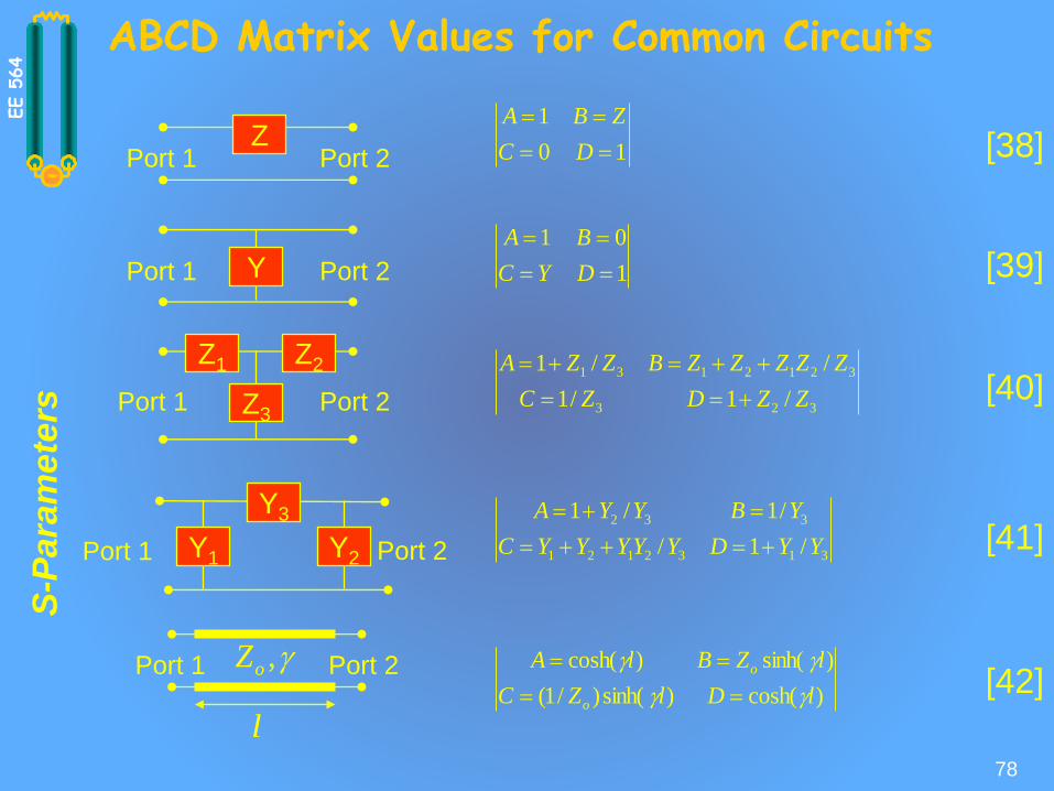
ABCD Matrix Values for Common Circuits
78
ZPort 1 Port 2 10
1
DC
ZBA
Port 1 Y Port 2 1
01
DYC
BA
323
3212131
/1/1
//1
ZZDZC
ZZZZZBZZA
Z1
Port 1 Port 2
Z2
Z3
Y1Port 1 Port 2Y2
Y3
3132121
332
/1/
/1/1
YYDYYYYYC
YBYYA
Port 1 Port 2,oZ)cosh()sinh()/1(
)sinh()cosh(
lDlZC
lZBlA
o
o
l
[38]
[39]
[40]
[41]
[42]

S-P
ara
mete
rsEE 5
64
Converting to and from the S-Matrix
The S-parameters can be measured with a VNA, and
converted back and forth into ABCD the Matrix
Allows conversion into a more intuitive matrix
Allows conversion to ABCD for cascading
ABCD matrix can be directly related to several useful circuit
topologies
79
S-P
ara
mete
rsEE 5
64
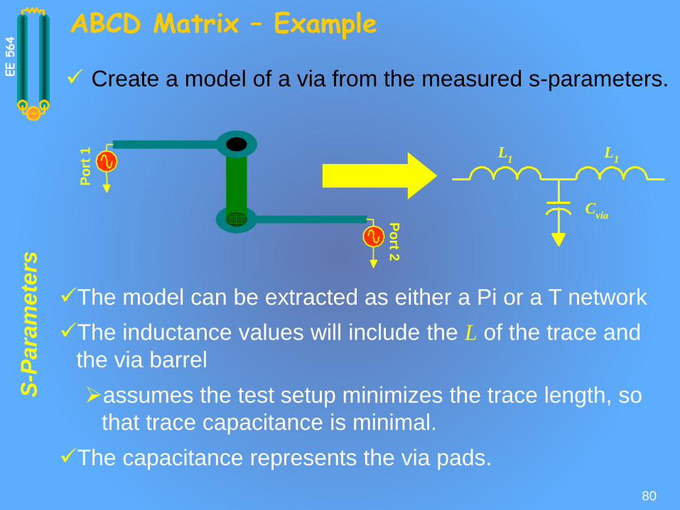
ABCD Matrix – Example
Create a model of a via from the measured s-parameters.
80
Po
rt 2
Po
rt 1
The model can be extracted as either a Pi or a T network
The inductance values will include the L of the trace and
the via barrel
assumes the test setup minimizes the trace length, so
that trace capacitance is minimal.
The capacitance represents the via pads.
L1
L1
Cvia

S-P
ara
mete
rsEE 5
64
ABCD Matrix – Example #1 The measured S-parameter matrix at 5 GHz is:
81
153.0110.0572.0798.0
572.0798.0153.0110.0
2221
1211
jj
jj
SS
SS
Converted to ABCD parameters:
827.00157.0
08.20827.0
2
11
2
11
2
11
2
11
21
21122211
21
21122211
21
21122211
21
21122211
j
j
S
SSSS
SZ
SSSS
S
SSSSZ
S
SSSS
DC
BA
VNA
VNA
Relating the ABCD parameters to the T circuit topology,
the capacitance can be extracted from C & inductance
from A:pFC
fCj
ZjC VIA
VIA
5.0
2
1
110157.0
3
nHLLfCj
fLj
Z
ZA
VIA
35.0)2/(1
21827.01 21
3
1
Z1
Port 1 Port 2
Z2
Z3

S-P
ara
mete
rsEE 5
64
Advantages/Disadvantages of ABCD Matrix
Advantages:
The ABCD matrix is intuitive: it describes all ports with
voltages and currents.
Allows easy cascading of networks.
Easy conversion to and from S-parameters.
Easy to relate to common circuit topologies.
Disadvantages:
Difficult to directly measure: Must convert from
measured scattering matrix.
82

S-P
ara
mete
rsEE 5
64
Summary
We can characterize interconnect networks
using n-Port circuits.
The VNA uses S- parameters.
From S- parameters we can characterize
transmission lines and discrete elements.
83
S-P
ara
mete
rsEE 5
64
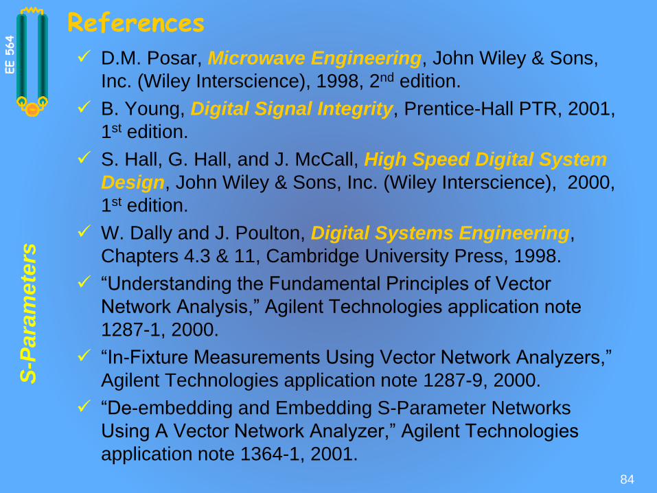
References D.M. Posar, Microwave Engineering, John Wiley & Sons,
Inc. (Wiley Interscience), 1998, 2nd edition.
B. Young, Digital Signal Integrity, Prentice-Hall PTR, 2001,
1st edition.
S. Hall, G. Hall, and J. McCall, High Speed Digital System
Design, John Wiley & Sons, Inc. (Wiley Interscience), 2000,
1st edition.
W. Dally and J. Poulton, Digital Systems Engineering,
Chapters 4.3 & 11, Cambridge University Press, 1998.
“Understanding the Fundamental Principles of Vector
Network Analysis,” Agilent Technologies application note
1287-1, 2000.
“In-Fixture Measurements Using Vector Network Analyzers,”
Agilent Technologies application note 1287-9, 2000.
“De-embedding and Embedding S-Parameter Networks
Using A Vector Network Analyzer,” Agilent Technologies
application note 1364-1, 2001.
84
S-P
ara
mete
rsEE 5
64
Appendix
More material on S parameters.
85

S-P
ara
mete
rsEE 5
64
86
0Re
any for 0Re
mn
mn
Y
m,nZ
jkkIj
iij
I
VZ
,0
jkkVj
iij
V
IY
,0
Lossless
Reciprocal jiij ZZ jiij ZZ
1 ZY
S-P
ara
mete
rsEE 5
64
S Parameters
87
NNNNN
N
N V
V
V
SSS
S
SSS
V
V
V
2
1
21
12
12111
2
1
VSV
jkkVj
iij
V
VS
,0
Scattering Matrix: S Parameters
or [1]
where [2]
nnn VVV
nnnnn VVIII ????
VVVIZIZIZ
VUZVUZ
10
10
001
U
UZUZVVS 11
S-P
ara
mete
rsEE 5
64
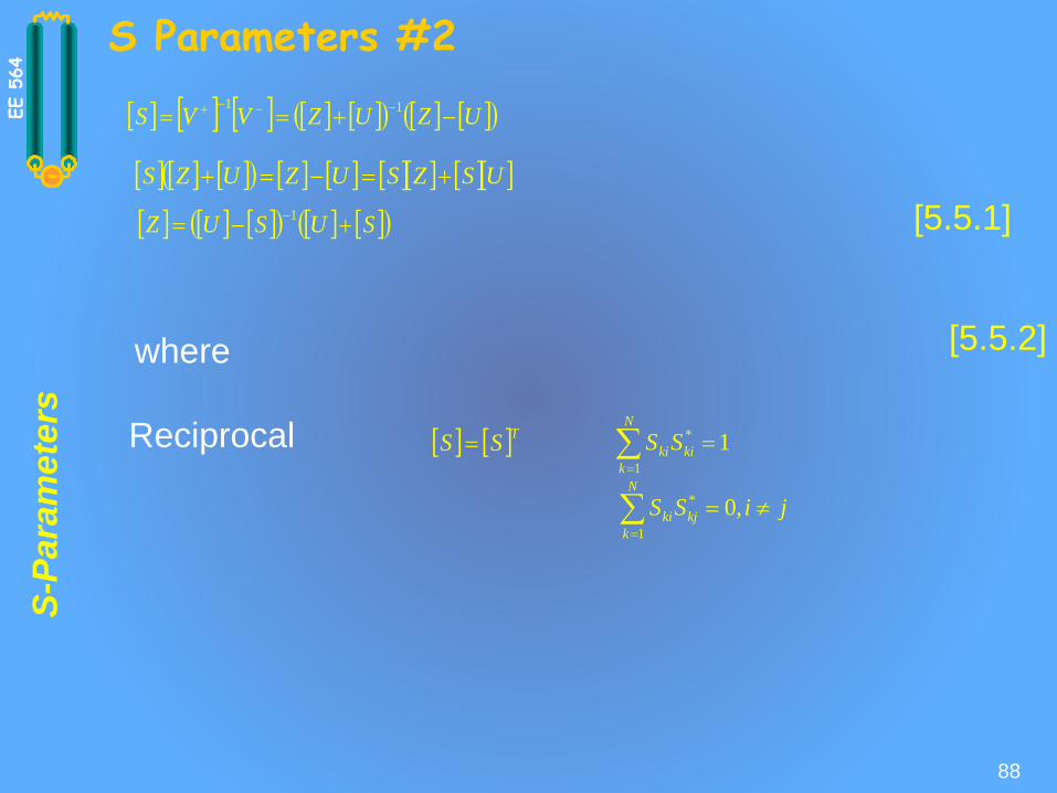
S Parameters #2
88
[5.5.1]
where [5.5.2]
UZUZVVS 11
USZSUZUZS
SUSUZ 1
TSS Reciprocal
N
k
kikiSS1
* 1
N
k
kjki jiSS1
* ,0
S-P
ara
mete
rsEE 5
64
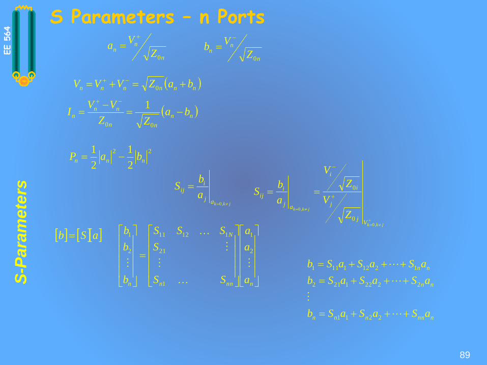
S Parameters – n Ports
89
n
nn
Z
Va
0
aSb
n
nn
Z
Vb
0
nnnnnn baZVVV
0
nn
nn
nnn ba
ZZ
VVI
00
1
22
2
1
2
1nnn baP
jkkaj
iij
a
bS
,0
jkk
jkk
Vj
j
i
i
aj
iij
Z
V
Z
V
a
bS
,0
,0
0
0
nnnn
N
n a
a
a
SS
S
SSS
b
b
b
2
1
1
21
11211
2
1
nnnnnn
nn
nn
aSaSaSb
aSaSaSb
aSaSaSb
2211
22221212
12121111

S-P
ara
mete
rsEE 5
64
S Parameters #4
90
aSb
where
jkkaj
iij
a
bS
,0
jkk
jkk
Vj
j
i
i
aj
iij
Z
V
Z
V
a
bS
,0
,0
0
0
niaSbn
j
jiji ,,3,2,1for
Sij = Gij is the reflection coefficient of the ith
port if i=j with all other ports matched
Sij = Tij is the forward transmission coefficient
of the ith port if I>j with all other ports
matched
Sij = Tij is the reverse transmission coefficient
of the ith port if I<j with all other ports
matched

S-P
ara
mete
rsEE 5
64
VNA Calibration
Proper calibration is critical!!!
There are two basic calibration methods
Short, Open, Load and Thru (SOLT)
• Calibrated to known standard( Ex: 50)
• Measurement plane at probe tip
Thru, Reflect, Line(TRL)
• Calibrated to line Z0
– Helps create matched port condition.
• Measurement plane moved to desired position set by
calibration structure design.
91

S-P
ara
mete
rsEE 5
64
SOLT Calibration Structures
92
OPEN SHORT
LOAD THRU
Calibration Substrate
G
G
S
S
G
S
Signal
Ground
G
S
G
S
S-P
ara
mete
rsEE 5
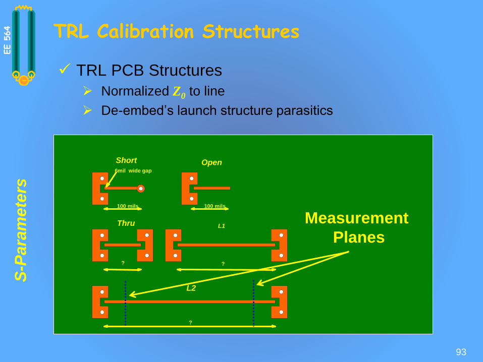
64 TRL Calibration Structures
TRL PCB Structures
Normalized Z0 to line
De-embed’s launch structure parasitics
93
6mil wide gap
Short
100 mils 100 mils
Open
?
Thru
?
L1
?
L2
Measurement
Planes
S-P
ara
mete
rsEE 5
64
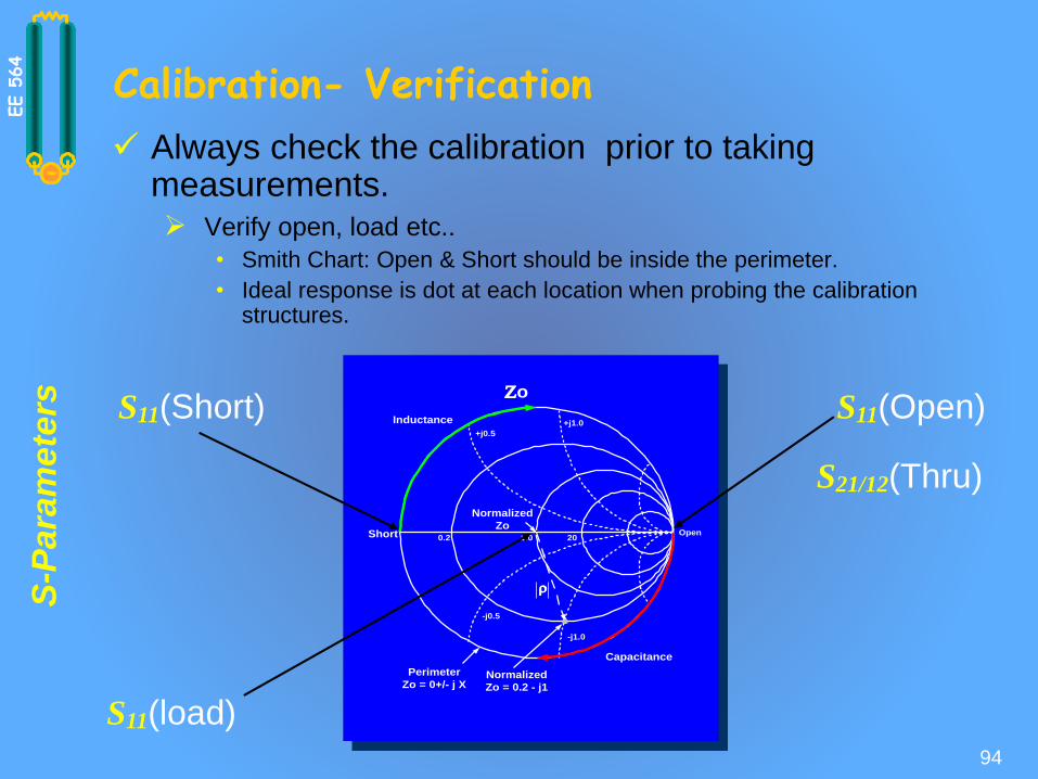
Calibration- Verification
Always check the calibration prior to taking measurements. Verify open, load etc..
• Smith Chart: Open & Short should be inside the perimeter.
• Ideal response is dot at each location when probing the calibration structures.
94
Capacitance
Inductance
Normalized
Zo
Perimeter
Zo = 0+/- j X
Short 1.00.2 20
-j0.5
-j1.0
+j0.5
+j1.0
Zo
Open
Normalized
Zo = 0.2 - j1
S11(Short) S11(Open)
S11(load)
S21/12(Thru)

S-P
ara
mete
rsEE 5
64
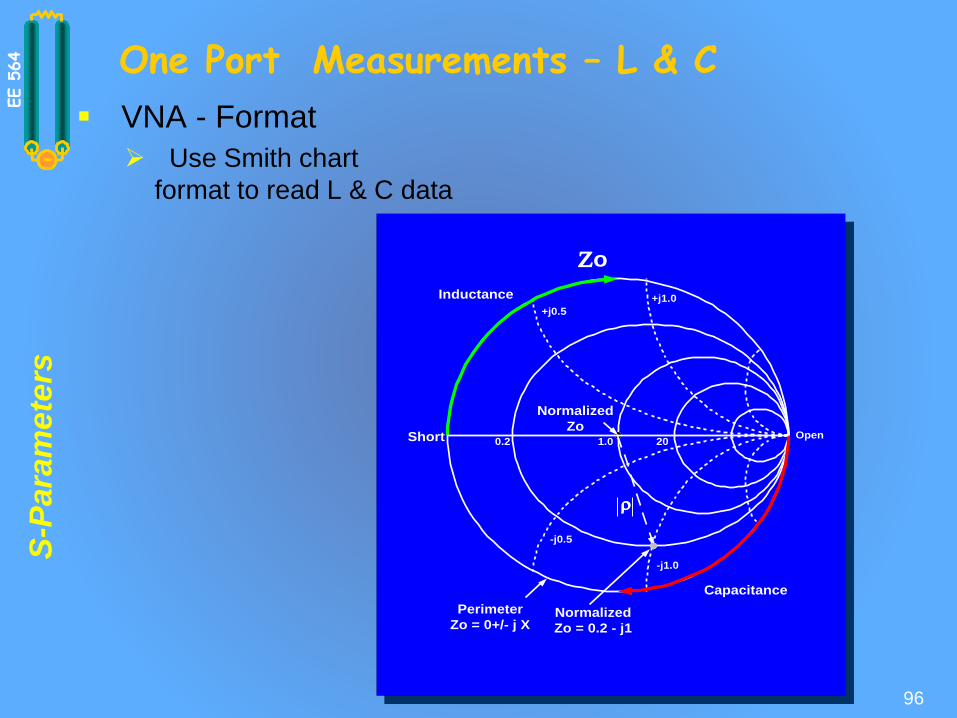
One Port Measurements
Practical sub 2 GHz technique for L & C data.
Structure must be electrically shorter than /4 of fmax.
1st order (Low Loss):
• Zin = jL (Shorted transmission line)
• Zin = 1/jC (Open transmission line)
• For an electrically short structure V and I to order are ~constant.
At the short, we have Imax and Vmin.
Measure L using a shorted transmission line with negligible loss.
At the open you have Vmax and Imin.
Measure C using an open transmission line with negligible loss.
95
V
RS= 50 DUT Short
CurrentZin = jL·I
DUT
Open
V
RS = 50
Zin = V/jC
S-P
ara
mete
rsEE 5
64 One Port Measurements – L & C
VNA - Format
Use Smith chart
format to read L & C data
96
Capacitance
Inductance
Normalized
Zo
Perimeter
Zo = 0+/- j X
Short 1.00.2 20
-j0.5
-j1.0
+j0.5
+j1.0
Zo
Open
Normalized
Zo = 0.2 - j1
S-P
ara
mete
rsEE 5
64
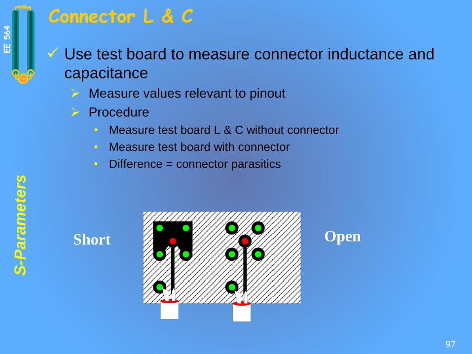
Connector L & C
Use test board to measure connector inductance and
capacitance
Measure values relevant to pinout
Procedure
• Measure test board L & C without connector
• Measure test board with connector
• Difference = connector parasitics
97
Short Open