universidad nacional del surmates dr. tobias “the dude” hidalgo-stitz, m.sc. ahmet hasim...
TRANSCRIPT


Tampereen teknillinen yliopisto. Julkaisu 984 Tampere University of Technology. Publication 984
Ali Shahed hagh ghadam Contributions to Analysis and DSP-based Mitigation of Nonlinear Distortion in Radio Transceivers Thesis for the degree of Doctor of Technology to be presented with due permission for public examination and criticism in Tietotalo Building, Auditorium TB109, at Tampere University of Technology, on the 21st of October 2011, at 12 noon. Tampereen teknillinen yliopisto - Tampere University of Technology Tampere 2011

Supervisor Mikko Valkama, Dr. Tech., Professor Department of Communications Engineering Tampere University of Technology Tampere, Finland Pre-examiners Fernando H. Gregorio, Dr. Tech., Assistant Professor Department of Electrical Engineering and Computers Universidad Nacional del Sur Bahia Blanca, Argentina Ali M. Niknejad, Ph. D., Associate Professor Department of Electrical Engineering and Computer Sciences University of California-Berkeley Berkeley, USA Opponent Markku Juntti, Dr. Tech., Professor Department of Electrical and Information Engineering University of Oulu Oulu, Finland ISBN 978-952-15-2650-3 (printed) ISBN 978-952-15-2794-4 (PDF) ISSN 1459-2045
ABSTRACT
This thesis focuses on different nonlinear distortion aspects in radio transmit-ter and receivers. Such nonlinear distortion aspects are generally becomingmore and more important as the communication waveforms themselves getmore complex and thus more sensitive to any distortion. Also balancingbetween the implementation costs, size, power consumption and radio per-formance, especially in multiradio devices, creates tendency towards usinglower cost, and thus lower quality, radio electronics. Furthermore, increasingrequirements on radio flexibility, especially on receiver side, reduces receiverradio frequency (RF) selectivity and thus increases the dynamic range andlinearity requirements. Thus overall, proper understanding of nonlinear dis-tortion in radio devices is essential, and also opens the door for clever use ofdigital signal processing (DSP) in mitigating and suppressing such distortioneffects.
On the receiver side, the emphasis in this thesis is mainly on the analysisand DSP based compensation of dominant intermodulation distortion (IMD)effects in wideband direct-conversion receiver (DCR). The DCR structure isstudied in the context of wideband flexible radio type of concepts, such assoftware-defined radio (SDR) and cognitive radio (CR), where minimal se-lectivity filtering is performed at RF. A general case of wideband receivedwaveform with strong blocking type signals is assumed, and the exact IMDprofile on top of the weak signal bands is first derived, covering the nonlinear-ities of low-noise amplifier (LNA) as well as the small-signal components, likemixers and amplifiers in the in-phase (I) and quadrature-phase (Q) branchesof the receiver. Stemming from the derived interference profiles, a versatileDSP-based adaptive interference cancellation (IC) structure is then proposedto mitigate the dominant IMD components at the weak signal bands. Fur-thermore, the issue of RF-local oscillator (LO) leakage in mixers is addressedin detail, creating in general both static as well as dynamic direct current(DC) offset type of interference at the desired signal band. Using properreceiver and signal modeling, a blind DSP-based method building on inde-pendent component analysis (ICA) is then proposed for suppressing such

iv Abstract
interference, especially due to strong blocking signals, in multi-antenna di-versity receivers. Altogether, both computer simulations as well as measuredreal-world radio signals are used to verify and demonstrate the operation ofthe proposed algorithms.
On the transmitter side, the major source on nonlinearity in radio devicesis the RF power amplifier (PA). In general, nonlinear PAs possess superiorpower efficiency compared to linear PAs, but generate also interfering spuri-ous distortion components at the transmitter output. Methods to mitigatesuch interference, both in-band and out-of-band, also known as linearizers,are highly active research area, and is also the second main theme of thisdissertation manuscript. More specifically, the work in this thesis focuses onthe so-called feedforward (FF) PA linearizer, which is building on identifyingand subtracting the spurious frequency components at and around the PAoutput. Such FF linearizer can in principle handle wideband transmit wave-forms and PA memory, but is also basically sensitive to certain componentmismatches in the linearization loops. In this thesis, a closed-form expressionrelating such component inaccuracies and the achievable linearization perfor-mance is derived, being applicable with both memoryless core PAs and corePAs with memory. Furthermore, as one of the main thesis contributions, aso-called DSP-oriented feedforward linearizer (DSP-FF) is proposed in thisthesis, which is a versatile implementation where the core of the lineariza-tion signal processing is carried out in digital domain at low frequencies,opposed to more traditional all-RF linearizers. Also efficient parameter esti-mation algorithms are derived for the proposed DSP-FF structure, buildingon least-squares (LS) model fitting and widely-linear (WL) filtering. Further-more, the large sample performance of the proposed parameter estimationmethods, and there on of the overall linearizer in terms of the achievable IMDattenuation, are derived covering both memoryless PAs and PAs with mem-ory. Overall, extensive computer simulations as well as proof-of-concept typeradio signal measurements are used to demonstrate and verify the analysisresults as well as the proper operation of the overall linearizer.
PREFACE
This manuscript is the outcome of the studies and research conducted at theDepartment of Communications Engineering (DCE) at Tampere Universityof Technology (TUT), Finland. This work was financially sponsored by Doc-toral program in Information Science and Engineering (formerly known asTampere Graduate School in Information Science and Engineering (TISE)),the Academy of Finland (under the projects “Understanding and Mitigationof Analog RF Impairments in Multi-Antenna Transmission Systems” and“Digitally-Enhanced RF for Cognitive Radio Devices”), the Finnish FundingAgency for Technology and Innovation (Tekes; under the projects “AdvancedTechniques for RF Impairment Mitigation in Future Wireless Radio Systems”and “Enabling Methods for Dynamic Spectrum Access and Cognitive Ra-dio”), the Technology Industries of Finland Centennial Foundation, AustrianCenter of Competence in Mechatronics (ACCM), Nokia Siemens Networks(formerly Nokia Networks), the Nokia Foundation, Tekniikan edistamissaatio(TES), and the Tuula and Yrjo Neuvo Foundation .
I have been extremely lucky to enjoy the company of many brilliant peoplein my life that helped me through the highs and lows of my academic careerthus far. Interaction with this amazing bunch shaped not only the directionof my scientific career but the human being I am today. My supervisor, Prof.Mikko Valkama taught me to aim for excellence no matter how impossible anddifficult. I express my gratitude for the opportunity he provided me to workunder his supervision. I am deeply grateful for his help, guidance, supportand patience during my research work. Prof. Markku Renfors, who acceptedme into DCE family as a young, inexperienced researcher and supervisedme with my M.Sc. research topic, taught me how to trust people and bringthe best out of them. I am also grateful of my M.Sc. co-supervisor Prof.Tapio Saramaki who introduced me to the concept of controlled insanity inscientific research.
I would like to thank Prof. Andreas Springer, from Institute for Com-munications and Information Engineering at Johannes Kepler University ofTechnology, Linz Austria for his hospitality during my research visit to Jo-

vi Preface
hannes Kepler University during summer of 2009. I am also grateful of Dr.Gernot Hueber, former member of the RF innovation group at Danube In-tegrated Circuit Engineering GmbH & Co KG (DICE), for providing mewith the opportunity to work alongside him during the summer of 2009. Myspecial thanks also goes to M.Sc. Sascha Burghlechner not only for fruit-ful collaboration on topics included in this manuscript but for being such aamazing company throughout my stay in Linz. Meanwhile, I should thankM.Sc. Marcelo Bruno for fruitful collaborations we had during his exchangevisit to DCE.
I would like to express deep gratitude to my thesis pre-examiners Assoc.Prof. Ali M. Niknejad from UC-Berkeley, USA, and Asst. Prof. Fernando H.Gregorio from Universidad Nacional del Sur, Argentina, for their insightfulcomments which opened fascinating perspectives on different topics of thedissertation for me and greatly improved the final manuscript. I also wouldlike to thank Prof. Markku Juntti from University of Oulu, Finland, foragreeing to act as opponent in my dissertation defense.
I would like to thank all my colleagues for the pleasant and friendly workenvironment in DCE/DTG. Meanwhile, I extend my special thanks to my col-leagues in RF-DSP group Dr. Lauri Anttila, Dr. Yaning Zou, M.Sc. AhmetHasim Gokceoglu, M.Sc. Adnan Kiayani, M.Sc. Jaakko Marttila, M.Sc. VilleSyrjala, M.Sc. Markus Allen and M.Sc. Nikolay N. Tchamov for brilliant dis-cussions on the topic of dirty-RF in various occasions and for direct/indirectcontribution to my research work as a whole. I also should thank Ulla Sil-taloppi, Coordinator of International Education and Elina Orava, Coordi-nator of International Education in Computing and Electrical EngineeringFaculty (CEE), for their tremendous assistance on everyday matters whichmake life for foreign researchers, like me, less stressful. Also tremendousgratitude toward past and present DCE administrative staff Tarja Eralaukko,Kirsi Viitanen, Sari Kinnari, Daria Ilina and Marianna Jokila for putting upwith my constant need for assistance in bureaucratic matter with unlimitedpatience.
In a more personal level, I would like to thank my past and present officemates Dr. Tobias “the dude” Hidalgo-Stitz, M.Sc. Ahmet Hasim Gokceoglu,M.Sc. Eero Maki-Esko and M.Sc. Andreas Hernandez for making TG113 thebest office in the entire campus. Also, I would like to extend my appreciationto Iranian community in TUT for creating a slice of heart-warming familiarityfaraway from home.
My heart-felt gratitude and love to my parents Asghar and Mehri forthey provided me with a nurturing environment at home and allowed me toexperiment my way through life. I am grateful to grow up with Leily andHaleh, two of the best and funnest sisters one could wish for. And last, butnot least, I would like express my genuine and heart-felt love and appreci-ation to my lovely wife Baharak “nafas” Soltanian and my sweet son Alan

vii
“jigar” Shahed hagh ghadam for making our house feel like home, for theirunconditional love and passion, and for the joy they bring to my life.
Ali Shahed hagh ghadamTampere, October 2011.

viii Preface

CONTENTS
Abstract iii
Preface v
List of Publications xi
List of Essential Symbols and Abbreviations xiii
Symbols . . . . . . . . . . . . . . . . . . . . . . . . . . . . . . . . . xiii
Abbreviations . . . . . . . . . . . . . . . . . . . . . . . . . . . . . . xviii
1 Introduction 1
1.1 Motivation and Background . . . . . . . . . . . . . . . . . . . 1
1.2 Scope of the Thesis: Nonlinear Distortion in Radios . . . . . . 2
1.3 Outline and Main Contributions of the Thesis . . . . . . . . . 7
2 Nonlinear Distortion Effects in Direct-conversion Receivers 11
2.1 I/Q Processing Principles . . . . . . . . . . . . . . . . . . . . 11
2.2 Spurious Frequency Profiles for Even- and Odd-Order Nonlin-earities . . . . . . . . . . . . . . . . . . . . . . . . . . . . . . . 14
2.3 Inter/Cross-modulation Distortion in Direct-conversion Re-ceivers . . . . . . . . . . . . . . . . . . . . . . . . . . . . . . . 19
3 Digital Cancellation of Intermodulation in Direct-conversionReceivers 29
3.1 Basics of Interference Canceller Operation . . . . . . . . . . . 29
3.2 Computer Simulation and Laboratory Measurement Examples 38

x Contents
4 Digital Mitigation of Dynamic Offset in Diversity Receivers 454.1 Modeling Dynamic Offset in Diversity Receiver . . . . . . . . 454.2 Spatial Processing Methods . . . . . . . . . . . . . . . . . . . 46
5 Nonlinearity Modeling and Linearization Techniques in Ra-dio Transmitters 555.1 Characterizing Input/Output Relation in RF PA . . . . . . . 565.2 Linearization Techniques . . . . . . . . . . . . . . . . . . . . . 62
6 Operation and Sensitivity Analysis of Feedforward PA Lin-earizer 676.1 Feedforward linearizer Operation Principle . . . . . . . . . . . 676.2 Linearizer Performance Under the SC and EC Coefficient Errors 68
7 DSP-oriented Feedforward Amplifier Linearizer 757.1 DSP-FF Basic Operation Principle . . . . . . . . . . . . . . . 757.2 Least-Squares Methods for SC and EC Coefficient Estimation 807.3 DSP-FF Linearization Performance Analysis . . . . . . . . . . 837.4 Simulation and Numerical Examples . . . . . . . . . . . . . . 86
8 Conclusions 97
9 Summary of Publications and Author’s Contributions 1019.1 Summary of Publications . . . . . . . . . . . . . . . . . . . . . 1019.2 Author’s Contributions to the Publications . . . . . . . . . . . 102
Appendix 105A.1 Real Bandpass Nonlinearity . . . . . . . . . . . . . . . . . . . 105A.2 I/Q Bandpass Nonlinearity . . . . . . . . . . . . . . . . . . . . 107
Bibliography 113

LIST OF PUBLICATIONS
This Thesis is mainly based on the following publications.
[P1] M. Valkama, A. Shahed hagh ghadam, L. Antilla and M. Renfors, “Ad-vanced digital signal processing techniques for compensation of nonlin-ear distortion in wideband multicarrier radio receivers,” IEEE Trans.Microw. Theory Tech., vol. 54, issue 6, Part 1, June 2006, pp. 2356 -2366
[P2] A. Shahed hagh ghadam, S. Burglechner, A. H. Gokceoglu, M. Valkama,and A. Springer, “Implementation and performance of DSP-orientedfeedforward power amplifier linearizer,” To appear in IEEE Trans. Cir-cuits Syst. I: Regular Papers, vol.59, issue 2, 2012.
[P3] A. Shahed hagh ghadam, T. Huovinen, M. Valkama, “Dynamic off-set mitigation in diversity receivers using ICA,” in proc. IEEE Int.Symp. Personal, Indoor and Mobile Radio Communications (PIMRC),Athens, Greece, Sep. 2007, pp. 1 - 5
[P4] A. Shahed hagh ghadam, M. Valkama, M. Renfors, “Adaptive com-pensation of nonlinear distortion in multicarrier direct-conversion re-ceivers,” in proc. IEEE Radio and Wireless Symp.(RAWCON), At-lanta, GA, USA, Sep. 2004, pp. 35-38.
[P5] A. Shahed hagh ghadam, A. H. Gokceoglu, M. Valkama, “Coefficientsensitivity analysis for feedforward amplifier linearizer with memory,”in Proc. Int. Symp. Wireless Personal Multimedia Communications(WPMC), Saariselka, Finland, Sep. 2008, .
[P6] S. Burglechner, A. Shahed hagh ghadam, A. Springer, M. Valkama, G.Hueber, “DSP-oriented implementation of feedforward power amplifierlinearizer,” in Proc. IEEE Int. Symp. Circuits and Systems (ISCAS),Taipei, May 2009, pp. 1755-1758.

xii List of Publications

LIST OF ESSENTIAL SYMBOLSAND ABBREVIATIONS
Symbols
A matrix containing SC circuit coefficients for DSP-FFALS,γ matrix containing LS-estimated SC circuit coefficients in
presence of measurement noiseA∞LS,γ matrix containing large sample LS-estimated SC circuit co-
efficients in presence of measurement noise
Awh,∞LS matrix containing large sample LS-estimated SC circuit co-
efficients (Wiener-Hammerstein core PA)Aopt matrix containing optimum SC circuit coefficients for DSP-
FFAwhopt Aopt for Wiener-Hammerstein core PA
A(t),A0(t),A1(t),A2(t) envelope of complex baseband signalsa1,a2,a3 polynomial coefficients for passband nonlinearityB matrix containing EC circuit coefficients in DSP-FFBopt matrix containing optimum EC circuit coefficients in DSP-FFb1,b2,b3 polynomial coefficients for in-phase branch nonlinearity
modeld(t) intermodulation component in Bussgang theoryf0,f1,f2 center frequencies of RF signalsf[.] nonlinear function in EASI
f0,f1,f2 center frequencies of signals after downconversionGLNA LNA gain in dBg1b1, g2b2, g3b3 polynomial coefficients for quadrature branch nonlinearityg[.] static nonlinearity behavioral modelge power gain of error amplifier Ge
hID(n),hIR(n) impulse responses of the main and reference path bandsplit
filters (in-phase branch)
xiv List of Essential Symbols and Abbreviations
hQD(n),hQR(n) impulse responses of the main and reference path bandsplit
filters (quadrature branch)h1(t),h2(t) impulse responses of pre- and post-filters in Wiener-
Hammerstein modelHu mixing matrix for statistically independent signal sources
ui(t)hu,i mixing coefficient vectors for signal ui(t)I, In×n identity matrixIMk(ωi) kth-order intermodulation interference resulted from a signal
located at ωiIMDAr Intermodulation distortion attenuation ratioIMDA∞
r Intermodulation distortion attenuation ratio in case largesamples are used to estimate EC coefficients
IMDAwh,∞r IMDA∞
r for Wiener-Hammerstein core PAj
√−1
Kd matrix containing I/Q downconverter imbalance coefficientsin DSP-FF
Km matrix containing I/Q upconverter imbalance coefficients inDSP-FF
kd,1,kd,2 I/Q downconverter imbalance coefficients in DSP-FFkm,1,km,2 I/Q upconverter imbalance coefficients in DSP-FFlc power loss of the attenuator LclI ,lQ LO-RF cross-leakage coefficients for I and Q mixersM(t) EASI update matrixMα,Mβ number of samples which are used in the estimation of SC
and EC coefficientsnD(n), nR(n) complex-valued IMD terms in the main and reference path
after bandsplit filtersnD,I(n),nR,I(n) IMD terms in the main and reference path after bandsplit
filters (in-phase branch)nD,Q(n),nR,Q(n) IMD terms in the main and reference path after bandsplit
filters (quadrature branch)nD,I(n),nD,Q(n) IC adaptive filters reference signals in I and Q branch (gen-
eral)
n(2)D,I(n),n
(2)D,Q(n) IC adaptive filters reference signals in I and Q branch for
second-order nonlinearity
n(3)D,I(n),n
(3)D,Q(n) IC adaptive filters reference signals in I and Q branch for
third-order nonlinearityO all-zero matrixpin,pγ input calibrating signal and measurement noise powerpm,pd input and IMD terms power for core PA in DSP-FFp∞d,o IMD power at the DSP-FF output when large samples are
used to estimate EC coefficients
xv
pwh,∞d,o p∞d,o for Wiener-Hammerstein core PApxu(t) desired signal power at the mixer input in dynamic DC-offset
mitigation casepxb(t) blocker signal power at RF LNA input in dynamic DC-offset
mitigation casepxb(t)(ICA) maximum allowable power of the RF blocker interference in
ICA-based compensation casepxb(t)(MRC) maximum allowable power of the RF blocker interference in
MRC-based compensation casep|xb(t)|2(ICA) maximum allowable power of the dynamic offset interference
in ICA-based compensation casep|xb(t)|2(MRC) maximum allowable power of the dynamic offset interference
in MRC-based compensation caseRu covariance matrix for desired signal mixing coefficient vector
hu,iR′u covariance matrix for interference signals mixing coefficient
vectors hu,j|j =ir-SIR ratio between the SIRo and SIRa
r-SIRWiener ratio between the SIRo and SIRa (Wiener core PA)SIRa SIR at the core PA output in feedforward linearizerSIRo SIR at feedforward linearizer outputSIRa−Wiener SIR at the core PA output in feedforward (Wiener core PA)SIRo−Wiener SIR at feedforward linearizer output (Wiener core PA)Ts sampling periodui(t) ith statistically independent signal sourceVa,iq,va,iq matrix and vector containing samples of va,iq(n)Vd,vd matrix and vector containing samples of vd(n)Vde,vde matrix and vector containing samples of vde(n)Ve,ve matrix and vector containing samples of ve(n)Ve,opt,ve,opt matrix and vector containing samples of ve,opt(n)Vin,vin matrix and vector containing samples of vin(n)Vout,vout matrix and vector containing samples of vout(n)Vm,vm matrix and vector containing samples of vm(n)Vγ,vγ matrix and vector containing samples of vγ(n)va,RF (t) the core PA RF output in DSP-FFva(t) baseband equivalent of the core PA output in feedforward
linearizerva(n) discrete-time baseband equivalent of the core PA output in
feedforward linearizerva,iq(n) I/Q downconverted version of the core PA output in DSP-FFvd,RF (t) IMD term at core PA output in DSP-FFvd(t) baseband equivalent of IMD term at the core PA output in
feedforward linearizer

xvi List of Essential Symbols and Abbreviations
vd(n) discrete-time baseband equivalent of IMD term at core PAoutput in feedforward linearizer
vde(n) discrete-time baseband equivalent of error amplifier outputin DSP-FF
ve(n) discrete-time baseband error signal in DSP-FFve,opt(n) discrete-time baseband error signal in DSP-FF given opti-
mum SC coefficientsvin(n) discrete-time baseband input calibrating signalvm,RF (t) the core PA RF input in DSP-FFvm(n) discrete-time baseband equivalent of core PA input in in feed-
forward linearizervm(t) baseband equivalent of core PA input in feedforward lin-
earizervo(t) baseband equivalent of feedforward linearizer outputvo(n) discrete-time baseband equivalent of feedforward linearizer
outputvout(n) discrete-time baseband output calibrating signalvγ(n) discrete-time baseband equivalent of measurement noisewI ,wQ IC adaptive filter coefficients vectors for I and Q branchesWD diversity (achieving) matrixWEASI(t) diversity (achieving) matrix for EASI algorithmwD,i ith column of WD
wi,I ,wi,Q IC adaptive filters ith coefficients for I and Q branchesxRF (t) bandpass RF signalxiq(t) I/Q downconverted version of signal xRF (t)x(t) complex baseband signalxI(t) in-phase component of signal x(t)xQ(t) quadrature component of signal x(t)xu(t) complex baseband version of the desired signalxb(t) complex baseband version of the blocker signalxD,I(t),xR,I(t) in-phase part of desired and reference signal before nonlin-
earityxD,Q(t),xR,Q(t) quadrature part of the desired and reference signals before
nonlineartyxD(t),xR(t) complex-valued desired and reference signals before nonlin-
earityxγ vector containing xγ,is for all the front-end branchesxγ,i zero-mean white Gaussian noise for ith front-end branchyRF (t) output of the bandpass nonlinearity modelyD,I(n),yR,I(n) signals of the main and reference pathes after bandsplit filters
(in-phase branch)yD,Q(n),yR,Q(n) signals of the main and reference pathes after bandsplit filters
(quadrature branch)

xvii
yD(t),yR(t) complex-valued desired and reference signals after nonlinear-ity
Z mixing matrix for dynamic DC-offset casezu,zb vectors containing channel coefficients for the desired signal
and blockers for receiver front-ends
ΛG matrix containing desired signal gain of the core PA in DSP-FF
α,α1,α2, SC circuit coefficientsα1,LS,α2,LS LS-estimated SC circuit coefficientsα∞1,LS,α
∞2,LS large sample size LS-estimated SC circuit coefficients
αopt,α1,opt,α2,opt SC circuit optimum coefficientsαG amplifier desired signal gainαLin amplifier linear gainαA(.) PA AM-AM transfer-functionβ,β1,β2, EC circuit coefficientsβ1,LS,β2,LS LS-estimated EC circuit coefficientsβ∞1,LS,β
∞2,LS large sample size LS-estimated EC circuit coefficients
βopt,β1,opt,β2,opt EC circuit optimum coefficientsϵ∞β,1,ϵ
∞β,2 error in the estimation of EC coefficients in large sample case
ϕ0(t),ϕ1(t),ϕ2(t) phase of complex baseband signalsψA(.) PA AM-PM transfer functionω0,ω1,ω2 angular center frequencies of RF signalsωu(t) angular center frequency of desired signal at RFωb(t) angular center frequency of blocker signal at RFω0,ω1,ω2 angular center frequencies of signals after downconversionµ IC adaptive filter step-sizeµEASI EASI algorithm step-sizeΣ∞B matrix containing errors in the estimation of EC coefficients
in large sample caseΥSNR,in matrix containing signal-to-measurement-noise ratio of the
input calibrating signal vin(n)
ΞIM/CMk kth-order non-interfering inter/cross-modulation components
ξα,ξβ normalized error in the SC and EC circuit coefficientsζu,i,ζb,i desired signal and blocker channel coefficients for receiver ith
front-end
≈ approximation|.| absolute value(.)∗ complex conjugate(.)T transposition

xviii List of Essential Symbols and Abbreviations
(.)H conjugate-transpose (Hermitian)(.)† matrix pseudoinverseE[.] statistical expectationRe[.] real part of complex signalIm[.] imaginary part of complex signal
Abbreviations
AC alternating currentACLR adjacent channel leakage ratioADC analog-to-digital converterAM-AM amplitude-to-amplitude modulationAM-PM amplitude-to-phase modulationAWGN additive white Gaussian noiseBPF bandpass filterCDMA code division multiple accessC/I carrier-to-interference ratioCR cognitive radioDAC digital-to-analog converterDC direct currentDCR direct-conversion receiverDLS data least-squaresDPD digital predistortionDSP digital signal processingDSP-FF DSP-oriented feedforward (linearizer)dB decibelEASI equivariant adaptive source identificationEC error cancellation (circuit)EVM error vector magnitudeFFT fast Fourier transformFIR finite impulse responseGHz gigaherzHPF highpass filterIBO input back-offIC interference cancellationICA independent component analysisIF intermediate frequencyIFFT inverse fast Fourier transformIMD intermodulation distortionI/Q in-phase and quadrature (parts of signal)LO local oscillatorLNA low-noise AmplifierLS least-squares
xix
LTE long-term evolutionMF matched filterM-GEF (SINR) maximizing generalized Eigen-gilterMHz megaherzMMF matrix matched filterMRC maximum ratio combiningNF noise figureOFDM orthogonal frequency division multiplexingP1dB 1 dB compression pointP3dB 3 dB compression pointPA power amplifierPAPR peak-to-average power ratioQAM quadrature amplitude modulationQPSK quadrature phase shift keyingRF radio frequencySC signal cancellation (circuit)SDR software-defined radioSER symbol error rateSINR signal-to-interference-and-Noise RatioSIR signal-to-interference ratioSNR signal-to-noise ratioSSPA solid-state power amplifierUMTS Universal Mobile Telecommunications SystemWH Wiener-HammersteinWJ Watkins JohnsonWL widely linearZF zero-forcing

xx List of Essential Symbols and Abbreviations

CHAPTER 1
INTRODUCTION
1.1 Motivation and Background
Throughout the years many application-specific radio standards have beendeveloped each optimized for a particular radio transmission scenario fromstationary close-range communication such as near-field communication (NFC)[1] to high-mobility long-range radio transmissions such as long-term evolu-tion (LTE) [2]. Nowadays, the state-of-the-art radio terminals are expectedto integrate many of these standards in one integrated and high performance,yet affordable and power efficient package which, in turn, introduces manychallenging constrains particularly in radio front-end design. These con-strains are becoming even more challenging with the recent trend towardmore flexible exploitation of available spectrum as introduced by paradigmshifting concepts such as cognitive radio (CR) [3, 4]. The receivers based onCR concept, for instance, are required to be wideband with high sensitivityand large dynamic range to be able to receive a weak desired signal in anyarbitrary frequency and in the presence of significantly stronger signals [5–7].As the result, the receiver analog front-end (Fig.1.1) of the CR should be im-plemented using linear and high quality analog components which results inrather expensive design with poor power efficiency. The CR transmitters, inturn, should be capable of transmitting at any arbitrary band through outthe spectrum and without interfering with the regulated radios [5,7]. Again,this can be obtained by deploying highly linear, yet expensive and powerin-efficient, analog components in the transmitter front-end (Fig.1.1). It isin these contexts that employing dirty-RF [8] concept is justified. The dirty-RF, in general, refers to a digital/mixed signal processing algorithm targetedat improving/correcting the performance of the analog front-end in the radiotransceivers. In particular, implementing dirty-RF-based algorithms for com-

2 Introduction
pensating the effects of nonlinearity in radio transceivers ease the linearityconstrains on the analog components of the radio transceivers which in turnresults in cheap yet high performance transceiver with excellent battery-life.
On the other hand, to design dirty-RF strategies for combating non-idealities in the transceiver front-end, including front-end nonlinearity, theeffects of the non-idealities should be fully explored and understood. There-fore, this manuscript aims to shed light on the different nonlinearity mecha-nisms, as the non-ideality under the focus of this manuscript, and their effectsin radio transceivers. Thereafter, based on the acquired knowledge, severaldirty-RF-based DSP algorithms are proposed to compensate the effects ofnonlinearity in the front-end of radio transceivers.
Figure 1.1: Wireless transmitter (left) and receiver (right) at conceptuallevel.
1.2 Scope of the Thesis: Nonlinear Distor-tion in Radios
1.2.1 Nonlinear Interference in Direct-Conversion Re-ceivers
Direct-conversion receiver (DCR) (Fig.1.2) is implemented based on the ideaof I/Q downconverting the desired radio frequency (RF) band directly to thebaseband. This is an alternative to superheterodyne receiver which down-converts the RF band of interest through multiple intermediate frequencies(IF). DCR eliminates the need for a number of off-chip elements, e.g. RF/IFimage rejection filters which are typically used in the superheterodyne re-ceivers [9, 10], and therefore suits better for monolithic designs. One closelyrelated structure to DCR is the low-IF [11,12] receiver concept. In this struc-ture the desired signal is I/Q downconverted directly to a low-IF frequencyand typically the conversion from low-IF to zero-frequency is performed inthe digital segment of the receiver. It is possible to view DCR as a specialcase of low-IF receiver where the IF frequency is actually zero [13]. Theline between the DCR and low-IF concept is particularly unclear in the con-text of multichannel receivers where multiple signals in different channels are
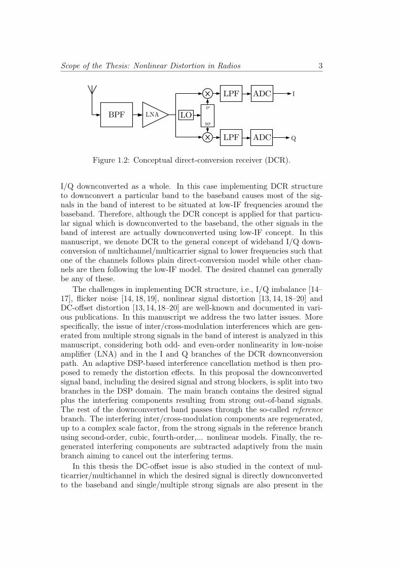
Scope of the Thesis: Nonlinear Distortion in Radios 3
Figure 1.2: Conceptual direct-conversion receiver (DCR).
I/Q downconverted as a whole. In this case implementing DCR structureto downconvert a particular band to the baseband causes most of the sig-nals in the band of interest to be situated at low-IF frequencies around thebaseband. Therefore, although the DCR concept is applied for that particu-lar signal which is downconverted to the baseband, the other signals in theband of interest are actually downconverted using low-IF concept. In thismanuscript, we denote DCR to the general concept of wideband I/Q down-conversion of multichannel/multicarrier signal to lower frequencies such thatone of the channels follows plain direct-conversion model while other chan-nels are then following the low-IF model. The desired channel can generallybe any of these.
The challenges in implementing DCR structure, i.e., I/Q imbalance [14–17], flicker noise [14, 18, 19], nonlinear signal distortion [13, 14, 18–20] andDC-offset distortion [13, 14, 18–20] are well-known and documented in vari-ous publications. In this manuscript we address the two latter issues. Morespecifically, the issue of inter/cross-modulation interferences which are gen-erated from multiple strong signals in the band of interest is analyzed in thismanuscript, considering both odd- and even-order nonlinearity in low-noiseamplifier (LNA) and in the I and Q branches of the DCR downconversionpath. An adaptive DSP-based interference cancellation method is then pro-posed to remedy the distortion effects. In this proposal the downconvertedsignal band, including the desired signal and strong blockers, is split into twobranches in the DSP domain. The main branch contains the desired signalplus the interfering components resulting from strong out-of-band signals.The rest of the downconverted band passes through the so-called referencebranch. The interfering inter/cross-modulation components are regenerated,up to a complex scale factor, from the strong signals in the reference branchusing second-order, cubic, fourth-order,... nonlinear models. Finally, the re-generated interfering components are subtracted adaptively from the mainbranch aiming to cancel out the interfering terms.
In this thesis the DC-offset issue is also studied in the context of mul-ticarrier/multichannel in which the desired signal is directly downconvertedto the baseband and single/multiple strong signals are also present in the

4 Introduction
downconverted band. The source of the DC-offset components is basicallythe lack of proper isolation in the mixer ports [13, 14, 18, 20] which, in turn,results in cross-leakage of RF and LO signals. These two phenomena, i.e.,leaking RF signal into LO path and vice versa, generate two distinct types ofDC-offset, namely dynamic and static. Both dynamic and static DC-offsetare analyzed in this manuscript. Particularly, the dynamic DC-offset, as themore challenging issue among the two, is the main focus of this manuscript.The dynamic DC-offset in a diversity receiver is analyzed. Moreover, a com-pensation scheme deploying higher order statistics based spatial processingis proposed to address this issue in the context of diversity receivers.
1.2.2 Earlier and Related Works
The issue of nonlinear distortion in the DCR has been studied in variousworks (e.g. [21–24]) prior to the publication of manuscript [P4]. In fact, thework presented in [P1] and [P4] can be viewed as a generalization of the ideasin [21] in which the focus is on cancelling only the second-order interferencein DCR structure. In [25] a hybrid analog-digital calibration technique hasalso been proposed which uses certain feedback from the receiver digital partsback to the analog sections. The feedback signal is used to adjust the I/Qmixer parameters in order to push down the observed nonlinear distortioncomponents. Since the publication of [P4] in 2004 and [P1] in 2006, severalextensions/variations of the proposed interference cancellation method hasbeen reported in literature, most notably [26–29]. The work reported in [26]deploys the proposed DSP cancellation method of [P1] and [P4] to mitigatethe cross-modulation distortion in the framework of software-defined radio(SDR) concept using a block based algorithm. In [27, 28] the interferencecancellation proposed in [P1] and [P4] is deployed to mitigate third-orderinterference terms stemming from strong signals in the band of interest fora universal mobile telecommunications system (UMTS) receiver. In this ap-proach the strong interference-generating signals are captured already afterthe LNA and the whole process of regenerating the third-order interferingterms are implemented in the analog domain rather than the DSP domainas is proposed in [P1] and [P4]. The extension of the work in [27, 28] formitigating higher order interference terms are reported in [29]. The same in-terference cancellation method is also proposed to compensate for nonlinearbehavior in ADC [30].
The problem of dynamic DC offset in direct conversion receivers andvarious solutions for this issue in single front-end context are reported invarious publications, e.g., [6, 13, 14,21,31,32]. Naturally, these solutions canbe applied for individual front-end branches in the case of multi-front-end(multi-antenna) receivers. However, as the number of front-end branchesincreases the cost of compensating for dynamic DC-offset accumulates pro-

Scope of the Thesis: Nonlinear Distortion in Radios 5
portionally. Therefore, devising a flexible and scalable DSP-based algorithm,such as the one proposed in [P3], to mitigate dynamic DC-offset in all thebranches of the multi-front-end (multi-antenna) receiver, is an attractive so-lution. One more important note on this topic is that the initial idea which isimplemented in [P3] lead to investigation on the performance of independentcomponent analysis (ICA) algorithm in noisy environments. The outcomesof this branch of study are reported in [33,34].
1.2.3 Transmitter Nonlinearity and Feedforward Lin-earization Technique
The main purpose of radio communication transmitter is to transmit the in-formation bearing signal to radio receiver while maximizing the data trans-fer considering the degrading effects in wireless medium e.g. channel noiseand fading. This should be achieved through parsimonious deployment ofresources such as spectrum and power with minimum interference to otherradio devices that are sharing the same medium. Current solutions to achievedesirable spectral efficiency partially involves exploiting high order symbol al-phabet and wideband multicarrier communications wave forms [35,36]. Thesewaveforms due to their high peak-to-average power ratio (PAPR) requirehighly linear power amplifier (PA) in the transmitter front-end [37, 38]. Onthe other hand, linear PAs by design have low power efficiency which in turnresults in poor overall power efficiency and excessive heat dissipation in radiotransmitters [39,40].
A prominent solution to enhance the power efficiency of a radio trans-mitter is to combine the use of nonlinear, and power efficient, PA and alinearizer. Linearization in general is a process in which the interferenceswhich are resulting from the nonlinear PA, i.e., intermodulation distortion(IMD) products, are mitigated through combination of additional circuitryand advanced (digital) signal processing algorithms. Feedforward linearizerin Fig. 1.3, as the focus of this manuscript, is one of the most establishedmethods of linearization. In short, the idea in feedforward linearization is tore-generate the interfering IMD products in signal cancellation (SC) circuitand subtract them from the final RF waveform in error cancellation (EC)circuit. In general, feedforward linearizer PA is unconditionally stable, PAmodel independent and particularly effective in wideband signal transmissionschemes with stringent linearity constrains [39, 41–45]. However, one of themain issues in feedforward structure is the vulnerability to any delay and/orgain mismatches between the upper and lower branches. Also any devia-tions in the linearizer coefficients α and β from their nominal values resultin linearizer performance degradation in general. The latter issue in feed-forward linearizer is analyzed [P5]. Particularly, as one of the contributionsof this thesis, the coefficients sensitivity analyses are extended to the case

6 Introduction
error cancellationsignal cancellation
G
Ge
Lc
vm( )t
va( )t
vo( )t
ve( )t
1
2
Figure 1.3: Baseband equivalent of feedforward power amplifier linearizerstructure.
where core PA exhibits memory effects [P5]. Another issue in implementingfeedforward linearizer is that it is commonly implemented entirely in the RFsegment of the transmitter. This results in a bulky and rigid design not soattractive for modern radio device concepts such as SDR and CR. In thismanuscript, we address this issue by proposing a DSP-oriented approach inimplementing the feedforward linearizer ([P2] and [P6]). In DSP-orientedfeedforward structure parts of the the EC and SC circuits are transferredto the DSP regime. Moreover, the calibration of EC and SC circuits areperformed independently and therefore the errors in the estimation of onecircuit do not affect the estimation of the other. This is certainly an advan-tage over sequential gradient based algorithms which are typically used forthe adaptation/calibration of all-RF feedforward linearizers [41,46,47]. Alsoclosed-form linearization performance analysis under large-sample conditionsis carried out for the overall linearizer concept.
1.2.4 Earlier and Related Works
Effects of misadjusting the feedforward linearizer coefficients in the overallperformance of this linearizer and for the case of the PA with instantaneousnonlinearity has been treated extensively in the literature [39, 41, 43]. Nev-ertheless, including the memory in the performance analysis, as one of thecontributions of this manuscript, enhances our understanding on the influ-ence of these coefficients in more generalized and practical settings. On thetopic of DSP-oriented feedforward linearizer (DSP-FF), few partially DSPbased implementations of feedforward linearizer have been reported to ad-dress the size and flexibility issues [48–53]. The proposals in [48, 50, 51, 53]generate the IMD components in DSP regime assuming certain behavioralmodel for the core PA. This approach delegates substantial part of the feed-

Outline and Main Contributions of the Thesis 7
forward linearizer functionality from RF to DSP and eliminates most of theRF components. However, the accuracy and the validity of the assumedbehavioral model for the core PA affects such linearizer performance. Theproposal in [49], in turn, attempts to compensate for the linear distortionsstemming from the RF components of feedforward linearizer already in thedigital baseband. This structure enhances the feedforward linearizer perfor-mance in wideband applications, but, the bulk of the feedforward linearizerin such structure is still implemented in the RF regime. In the structureof [52], the lower branch of the SC circuit is already implemented in thedigital domain. However, the EC circuit is still implemented in the RF do-main. The adaptation/calibration algorithm in this approach is based onsuccessive adaptation of the SC and EC circuits which is initially proposedin [41]. This calibration/adaptation method has the advantage of trackingthe possible circuit parameter changes without interrupting the transmission,while the transmitted signal is still degraded during the initial convergencetime. On the downside, this calibration/adaptation suffers from the estima-tion error propagation from SC to EC circuit. In other words, any estimationerror in the SC circuit, significantly deteriorate the estimation error in theEC circuit [41]. The estimation error propagation from SC to EC problem isaverted in the proposed structure in [P2] and [P6] by devising two indepen-dent least-squares-based estimation algorithm for SC and EC circuit.
1.3 Outline and Main Contributions of theThesis
In general this manuscript studies the effects of nonlinearity in radio trans-mitters and receivers front-ends. In Chapter 2 first the basics of I/Q signalprocessing is reviewed. This principle is the fundamental concept behind theoperation of DCR which is the focus of this manuscript. Thereafter, the spu-rious frequency profile of nonlinearities categorized in odd- and even-ordercases are presented. This analysis is performed using multi-tone input as wellas multiple modulated signals. The multi-tone characterization of a nonlin-ear element provides a clear picture on the frequencies of these componentsin comparison to the original input tone frequencies. On the other hand,the characterization of a nonlinear element using multiple modulated signalsprovides a broader view not only on the spectrum profile of the spurious fre-quency components but on their envelopes and phases which are particularlyimportant in understanding the true nature of the nonlinearity-born spu-rious components. It also creates a solid foundation for understanding andanalysis of the interference cancellation-based compensation method which isproposed in [P1] and [P4]. The spurious frequency profiles are also delineatedfor two distinct scenarios. One, multiple real-valued bandpass signals pass
8 Introduction
through odd- and even-order nonlinearities. The results of this study shedlight on the nonlinear behavior of such components as LNA. Two, multiplecomplex-valued bandpass signals pass through I and Q nonlinear compo-nents. Viewing the output spurious component profiles in this case fromcomplex-signal point of view reveals interesting differences comparing to thefirst case study which enhances our understanding of the nonlinear behav-ior of I/Q downconverters with nonlinear elements in their path. Examplespurious frequency components of such scenarios for three-signal scenario arederived in detail in the Appendix. The results of these derivations are usedthroughout the discussions in Chapters 2 and 3.
The final section of Chapter 2, describes the interference profile on topof the desired signal band stemming from nonlinearities in LNA, mixers andsubsequent stages of DCR. More precisely, a scenario in which the antennapicks up multiple strong signals, or blockers, within the same spectrum asthe weak desired signal is studied. The contributions of odd-order nonlinear-ity in LNA to the interference in desired signal band as the result of theseblockers are delineated. Special scenarios in which even-order nonlinearityin LNA contributes to the desired signal band interference are emphasized,most notably the role of even-order LNA nonlinearity for future widebandreceivers which are based on SDR and CR concepts. The contributions ofnonlinearity in the mixer and amplification stages of the I and Q branchesin DCR to the desired signal band interference profile are also studied inthis section. The final part of this section is dedicated to describing the DC-offset phenomenon in DCR as the result of finite isolations between mixingcore ports. Particularly, the difference between dynamic and static DC-offsetand the mechanisms which yield these offsets are explained and the signallevel expressions for both dynamic and static DC-offset are provided in thissection.
The basics and operation principle of the DSP-based adaptive interfer-ence cancellation method which is originally proposed in [P1] and [P4], arepresented in Chapter 3. This method is designed to mitigate the effects of thenonlinear inter/cross-modulation interfering products resulting from nonlin-ear LNA and nonlinear elements in I and Q branches of DCR downconversionpath through regenerating the interfering terms and adaptively subtractingthem from the nonlinear device output in a feedforward structure. The signallevel analysis of the proposed algorithm reveals the essential conditions underwhich this algorithm performs optimally. These conditions are examined andjustified using the three-signal example derivation provided in the Appendix.
Chapter 4 is dedicated to the issue of dynamic DC-offset in diversity re-ceivers. First, a signal model is developed for an example two-front-end DCRsuffering from dynamic DC-offset. It is shown that the optimal solution tomitigate the dynamic DC-offset is the spatial signal processing method thatachieves the maximum signal-to-interference-plus-noise ratio (SINR) such as

Outline and Main Contributions of the Thesis 9
SINR maximizing generalized Eigen-filter (M-GEF) [33,54,55]. However, theessential assumption in these algorithms is that the noise power and the chan-nel coefficients are known to the receiver. In the continuation of this chapterthe independent component analysis (ICA) based algorithm, which is ini-tially proposed in [P3], is described. This algorithm is capable of separatingthe desired signal from the dynamic DC-offset, up to scale and permutation,blindly. Thus no knowledge of the noise level and channel coefficients arerequired in this method. The SINR which is achieved by ICA-based methodis shown through computer simulation examples to be close to M-GEF-basedreceiver.
The basics and background of the nonlinearity characterization for RFPA are described in Chapter 5. The concept of behavioral modeling as asystem-level description of RF PA input-output relation is briefly discussed.Various widely used behavioral models for RF PA including Wiener, Ham-merstein and Wiener-Hammerstein models are introduced in this chapter.The linearization concept as a viable solution to the power efficiency andlinearity dilemma in RF PA is discussed. The digital predistortion (DPD) asa promising, yet developing, linearization method and feedforward linearizeras the most developed linearization technique are briefly described in thischapter.
The operation principle and signal models for feedforward linearizer aredescribed in detail in Chapter 6. Thereafter, the effects of misadjusting thefeedforward linearizer coefficients on linearization performance of this lin-earizer are studied. A measure called relative signal-to-interference ratio (r-SIR) [P5] is introduced as the ratio between signal-to-interference ratio (SIR)at the input of the PA and at the feedforward linearizer output. This mea-sure is then used to quantify the linearization performance of the feedforwardlinearizer. A unified expression for r-SIR in terms of errors in feedforwardlinearizer coefficients in the case of the memoryless core PA and in the casewhere the core PA exhibits memory is derived in this chapter.
A variation of feedforward structure, i.e., DSP-FF is introduced in Chap-ter 7. The basic operation and signal level models for this structure are pre-sented in this chapter. Thereafter, two independent block-based algorithmsare proposed for calibration of the SC and EC circuits. A closed-form expres-sion for the EC circuit coefficients estimation error is presented. In addition,a new measure for the performance analysis of DSP-FF is proposed. Thisfigure of merit, i.e., intermodulation distortion attenuation ratio (IMDAr), isdefined as the power ratio between the IMD at the PA and DSP-FF outputs.A closed form expression for IMDAr in terms of circuit parameters is derived.The analysis results are also extended for the case that the core PA exhibitsmemory effects. The closed form expressions for EC circuit coefficients es-timation and IMDAr as well as the DSP-FF gain analysis in this chapterfully describe the relation between the estimation errors in EC and SC and
10 Introduction
the linearization performance of DSP-FF. This, in fact, enables designers topredict the performance of DSP-FF analytically without the need for lengthysimulations.
A general conclusion on the topics discussed in this manuscript are drawnin Chapter 8. The summary of publications and author’s contributions tothe publications are included in Chapter 9.
All in all, the main purpose of this manuscript is to provide a plat-form to present the author’s contributions in [P1]-[P6] in a unified manner.From the receiver perspective, the contributions of the author are the overallnonlinearity-born interference analysis of the DCR downconversion chain inChapter 2, the adaptive IC method in Chapter 3 and the ICA-based DC-offset mitigation method in Chapter 4. The contributions of the author inanalyzing the effects of the errors in the SC and EC coefficients for all-RFfeedforward in the case of core PA with memory are included in Chapter 6.The entire Chapter 7 includes all the contributions of the author in proposing,signal-level analysis as well as performance analysis of DSP-FF. Naturally,more detailed information and analysis on the above mentioned topics areavailable in [P1]-[P6].

CHAPTER 2
NONLINEAR DISTORTIONEFFECTS IN
DIRECT-CONVERSIONRECEIVERS
2.1 I/Q Processing Principles
Understanding the true nature of bandpass signals and systems is the key inbuilding efficient radio transmitters and receivers. In addition to the basic en-velope and phase representation, the so called I/Q (in-phase/quadrature) in-terpretation forms the basis for various spectrally efficient modulation and de-modulation techniques [36]. And more generally, I/Q processing can be usedin the receiver and transmitter front-ends for efficient down/upconversionprocessing, independently of the applied modulation technique. Given ageneral bandpass signal
xRF (t) = 2Re[x(t)ejω0t] = x(t)ejω0t + x∗(t)e−jω0t (2.1)
= 2xI(t) cos(ω0t)− 2xQ(t) sin(ω0t)
= 2A(t) cos(ω0t+ ϕ(t))
the (formal) baseband equivalent signal x(t) is defined as
x(t) = A(t)ejϕ(t) = A(t) cos(ϕ(t)) + jA(t) sin(ϕ(t)) = xI(t) + jxQ(t) (2.2)
where A(t) and ϕ(t) denote the actual envelope and phase function, andthe corresponding I and Q signals appear as xI(t) = A(t) cos(ϕ(t)) andxQ(t) = A(t) sin(ϕ(t)), respectively. The baseband equivalent signal x(t)

12 Nonlinear Distortion Effects in Direct-conversion Receivers
2Re[ ( )exp( )]x t j tw0
LOWPASS
FILTER
cos( )w0t
-sin( )w0t
LOWPASS
FILTER
x t x tRe[ ( )]= ( )I
x t x tIm[ ( )]= ( )Q(b)
2Re[ ( )exp( )]x t j tw0LOWPASS
FILTERx t( )
(a)
exp( )- wj t0
Figure 2.1: Basic I/Q downconversion principle in terms of (a) complex sig-nals and (b) parallel real signals.
can be recovered by multiplying the modulated signal with a complex ex-ponential e−jω0t and lowpass filtering. This is illustrated in Fig. 2.1 whichalso depicts the practical implementation structure based on two parallel realsignals. In the receiver architecture context, the differences come basicallyfrom the interpretation of the downconverted signal structure. In general,both the direct-conversion [9, 13, 14, 18] and low-IF [9, 12] receivers utilizethe I/Q downconversion principle and are discussed in more detail in thefollowing. The so called DCR, also known as homodyne receiver, is based onthe idea of I/Q downconverting the channel of interest from RF directly tobaseband [9,13,14,18]. Thus in a basic single-channel context, the downcon-verted signal after lowpass filtering is basically ready for modulation-specificprocessing such as equalization and detection. On the other hand, low-IFreceiver [9,12], uses I/Q downconversion to a low but nonzero IF. Thus herea further downconversion from IF to baseband is basically needed before de-tection, depending somewhat on the actual data modulation. In the basicscenarios, this can be done digitally after sampling the signal at low inter-mediate frequency. In a wider context, with multiple frequency channels tobe detected, a generalization of the previous principles leads to a structurewhere the whole band of interest is I/Q downconverted as a whole. In thiscase, either the direct-conversion or low-IF model applies to individual chan-
I/Q Processing Principles 13
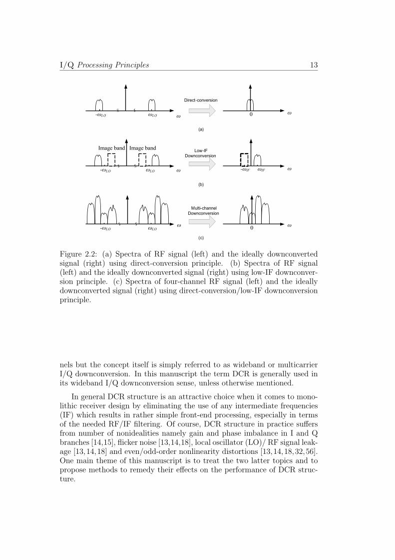
Figure 2.2: (a) Spectra of RF signal (left) and the ideally downconvertedsignal (right) using direct-conversion principle. (b) Spectra of RF signal(left) and the ideally downconverted signal (right) using low-IF downconver-sion principle. (c) Spectra of four-channel RF signal (left) and the ideallydownconverted signal (right) using direct-conversion/low-IF downconversionprinciple.
nels but the concept itself is simply referred to as wideband or multicarrierI/Q downconversion. In this manuscript the term DCR is generally used inits wideband I/Q downconversion sense, unless otherwise mentioned.
In general DCR structure is an attractive choice when it comes to mono-lithic receiver design by eliminating the use of any intermediate frequencies(IF) which results in rather simple front-end processing, especially in termsof the needed RF/IF filtering. Of course, DCR structure in practice suffersfrom number of nonidealities namely gain and phase imbalance in I and Qbranches [14,15], flicker noise [13,14,18], local oscillator (LO)/ RF signal leak-age [13,14,18] and even/odd-order nonlinearity distortions [13,14,18,32,56].One main theme of this manuscript is to treat the two latter topics and topropose methods to remedy their effects on the performance of DCR struc-ture.
14 Nonlinear Distortion Effects in Direct-conversion Receivers
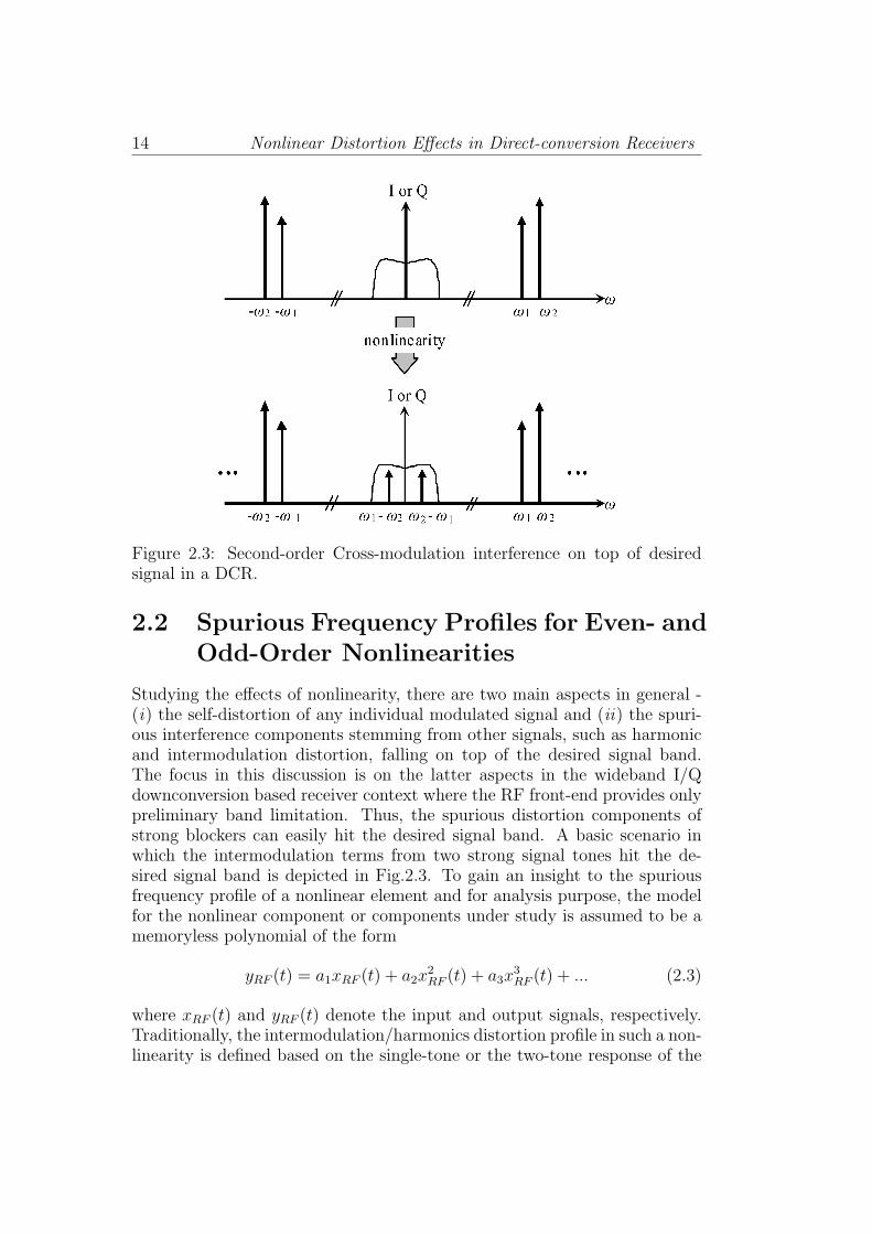
Figure 2.3: Second-order Cross-modulation interference on top of desiredsignal in a DCR.
2.2 Spurious Frequency Profiles for Even- andOdd-Order Nonlinearities
Studying the effects of nonlinearity, there are two main aspects in general -(i) the self-distortion of any individual modulated signal and (ii) the spuri-ous interference components stemming from other signals, such as harmonicand intermodulation distortion, falling on top of the desired signal band.The focus in this discussion is on the latter aspects in the wideband I/Qdownconversion based receiver context where the RF front-end provides onlypreliminary band limitation. Thus, the spurious distortion components ofstrong blockers can easily hit the desired signal band. A basic scenario inwhich the intermodulation terms from two strong signal tones hit the de-sired signal band is depicted in Fig.2.3. To gain an insight to the spuriousfrequency profile of a nonlinear element and for analysis purpose, the modelfor the nonlinear component or components under study is assumed to be amemoryless polynomial of the form
yRF (t) = a1xRF (t) + a2x2RF (t) + a3x
3RF (t) + ... (2.3)
where xRF (t) and yRF (t) denote the input and output signals, respectively.Traditionally, the intermodulation/harmonics distortion profile in such a non-linearity is defined based on the single-tone or the two-tone response of the

Spurious Frequency Profiles for Even- and Odd-Order Nonlinearities 15
nonlinearity in which the input of the nonlinearity are tone sinusoidal sig-nals. Excitement of such an element modeled by (2.3) with a blocker signalwith two frequency components, say ω1 and ω2, results in two groups of fre-quencies at the output - the harmonics of the form n× ω1 and m× ω2, andthe intermodulation (or cross-modulation) frequencies ±n × ω1 ± m × ω2,n,m = 1, 2, 3, ... as is well-known in the literature [10,19,57–61].
A more realistic spurious frequency profile of odd-/even-order nonlinear-ity from radio receivers perspective can be obtained using bandpass modu-lated signals as the input of the nonlinear component. In contrast to thepure-tone characterization method, these types of analysis provide informa-tion on the spurious components center frequencies as well as their envelopesand phases which is essential in understanding the nature of these terms asinterference. One example of such analysis is presented in detail in the Ap-pendix A.1. The provided analysis aim to motivate for understanding of theinter/cross-modulation profiles of devices such as LNA with mild nonlinear-ity. Therefore, the nonlinear elements up to third-order are considered in theanalysis. Moreover, the nonlinear component input xRF (t) consists of threebandpass signals at ω0, ω1 and ω2 which is defined as follows
xRF (t) = A0(t) cos(ω0t+ ϕ0(t)) + A1(t) cos(ω1t+ ϕ1(t))
+ A2(t) cos(ω2t+ ϕ2(t)) (2.4)
It is well-known in the literature, and it is also demonstrated in the AppendixA.1, that the second-order nonlinearity, i.e. x2RF (t), generates following typesof spurious components
• Around DCFor example a2
A20(t)
2,a2
A21(t)
2and a2
A22(t)
2
• At twice original signals frequencies
For example a2A2
0(t)
2cos(2ω0t+ 2ϕ0(t))
• Cross-modulations between signal pairsFor example a2A1(t)A2(t) cos
((ω1 + ω2)t+ ϕ1(t) + ϕ2(t)
)The third-order nonlinearity, i.e. x3RF (t), in turn, generates following inter/cross-modulation components
• Self-distortionsThese components hit the original signals center frequencies e.g.
a3(3A3
0(t)
4+
3A21(t)A0(t)
2+
3A22(t)A0(t)
2
)cos(ω0t+ ϕ0(t))
• At three-times original signals frequencies
For example a3A3
0(t)
4cos(3ω0t+ 3ϕ0(t))

16 Nonlinear Distortion Effects in Direct-conversion Receivers
• Cross-modulations between original signal pairs
For instance a33A2
1(t)A2(t)
4cos((2ω1 + ω2)t+ 2ϕ1(t) + ϕ2(t))
• Cross-modulations between all three of the original signals
For example a36A0(t)A1(t)A2(t)
4cos((ω1−ω2−ω0)t+ϕ1(t)−ϕ2(t)−ϕ0(t))
The above analysis can be extended, from complex I/Q signal perspective,when the nonlinearities take place in I/Q processing, like I/Q mixer. Anexample of such a scenario is provided in the Appendix A.2. Particularly,one should note that the referred derivations are designed to motivate theanalysis of the nonlinearity profile in scenarios in which I and Q branches of aDCR exhibit different, yet mild, nonlinearity. As the result, the nonlinearityin the I and Q branches are considered up to third-order elements only. Threecomplex signals at frequencies of ω0, ω1 and ω2 are assumed at the output ofthe I/Q downconverter. Note here that ω0, ω1 and ω2 can be considered asthe downconverted versions of ω0, ω1 and ω2, respectively. The input of thenonlinear element in this case can be written as follow
x(t) = xI(t) + jxQ(t) (2.5)
= A0(t)ej(ω0t+ϕ0(t)) + A1(t)e
j(ω1t+ϕ1(t)) + A2(t)ej(ω2t+ϕ2(t))
The overall complex spurious frequency profile stemming form I and Q com-ponents of the above signal passing through second-order nonlinearities inthe I and Q branches with distinct characteristics, i.e. b2x
2I(t) + jg2b2x
2Q(t),
can be categorized in following groups (refer to Table A.3 in Appendix).
• Components around DC
For example b2(1 + jg2)A2
0(t)
2, b2(1 + jg2)
A21(t)
2and b2(1 + jg2)
A22(t)
2
• At ±2-times original frequenciesFor example
b21−jg2
4
A20(t)
2ej(2ω0t+2ϕ0(t)) and b2
1−jg24
A20(t)
2e−j(2ω0t+2ϕ0(t))
• Cross-modulations of signal pairsFor exampleb2
1−jg22A1(t)A2(t)e
j((ω1+ω2)t+ϕ1(t)+ϕ2(t)) and
b21−jg2
2A1(t)A2(t)e
−j((ω1+ω2)t+ϕ1(t)+ϕ2(t))
One interesting observation here is that the second-order nonlinearity inthe form of b2x
2I + jg2b2x
2Q generates symmetric intermodulation and cross-
modulation components around zero frequency. This is true even in case ofdifferent characteristics in I and Q branch (g2 = 1) which results in the pres-ence of mirror frequencies components [15] on either side of the frequencyaxis.

Spurious Frequency Profiles for Even- and Odd-Order Nonlinearities 17
The overall complex spurious frequency profile stemming form I and Qcomponents of the signal in (2.5) passing through third-order nonlinearitieswith distinct characteristics, i.e. b3x
3I + jg3b3x
3Q, can, in turn, be categorized
in following groups (refer to Table A.4 in the Appendix).
• Self-distortionsOne example of such components is
b3(1+g3)2
(3A3
0(t)
4+
3A21(t)A0(t)
2+
3A22(t)A0(t)
2
)ej(ω0t+ϕ0(t))
• At ±3-times original frequenciesFor exampleb3(1+g3)
2
A30(t)
4e−j(3ω0t+3ϕ0(t)) and b3(1−g3)
2
A30(t)
4ej(3ω0t+3ϕ0(t))
• Cross-modulations of signal pairsFor exampleb3(1+g3)
2
3A21(t)A2(t)
4e−j((2ω1+ω2)t+2ϕ1(t)+ϕ2(t)) and
b3(1−g3)2
3A21(t)A2(t)
4ej((2ω1+ω2)t+2ϕ1(t)+ϕ2(t))
• Cross-modulations of all three signalsFor exampleb3(1+jg3)
26A0(t)A1(t)A2(t)
4e−j((ω1−ω2−ω0)t+ϕ1(t)−ϕ2(t)−ϕ0(t)) and
b3(1−jg3)2
6A0(t)A1(t)A2(t)4
ej((ω1−ω2−ω0)t+ϕ1(t)−ϕ2(t)−ϕ0(t))
Interestingly, the spurious frequency profile of the nonlinearity in the form ofb3x
3I + jg3b3x
3Q is not symmetric around the zero frequency. More precisely,
when the I and Q branches of the downconverter exhibit identical third-ordernonlinearities, the third-order inter/cross-modulation terms appear only atthe opposite side of the zero frequency comparing to the original signals. Forinstance, in the above example, given g3 = 1, the desired signal at ω0 gener-
ates the intermodulation termb3A3
0(t)
4e−j(3ω0t+3ϕ0(t)) but the intermodulation
term at the original signal side of the spectrum b3(1−g3)2
A30(t)
4ej(3ω0t+3ϕ0(t)) = 0.
Nevertheless, mismatch between the third-order characteristics of I and Qbranches creates extra inter/cross-modulation components at the same sideof the spectrum where the original signals are located. This is apparent in theabove example where, for instance, the third-order nonlinearities in I and Q
branches of the downconverter result in b3(1+g3)2
A30(t)
4e−j(3ω0t+3ϕ0(t)) as well as
b3(1−g3)2
A30(t)
4ej(3ω0t+3ϕ0(t)) when g3 = 1. There is also another crucial difference
compared to the earlier second-order nonlinearity, related to the spurious sig-nal component(s) at the original center-frequency ω0. While the second-ordercase is free from this ”self-distortion” such a spurious component is indeedthere in the third-order case.

18 Nonlinear Distortion Effects in Direct-conversion Receivers
Figu
re2.4:
Generic
schem
aticfor
DCR.This
figu
reis
detailed
todepict
thecom
pon
ents
contrib
utin
gto
odd-/even
-ord
ernon
linearity
interferen
ceprofi
le.
Inter/Cross-modulation Distortion in Direct-conversion Receivers 19
2.3 Inter/Cross-modulation Distortion in Direct-conversion Receivers
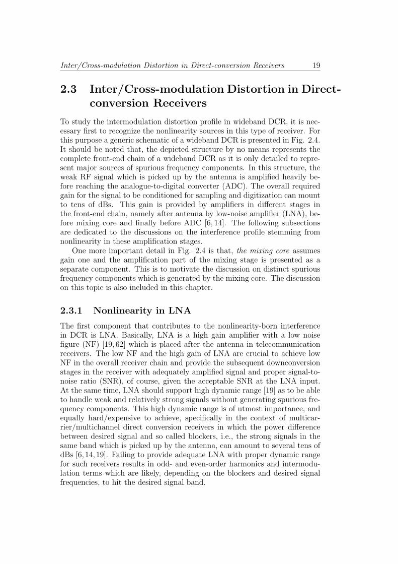
To study the intermodulation distortion profile in wideband DCR, it is nec-essary first to recognize the nonlinearity sources in this type of receiver. Forthis purpose a generic schematic of a wideband DCR is presented in Fig. 2.4.It should be noted that, the depicted structure by no means represents thecomplete front-end chain of a wideband DCR as it is only detailed to repre-sent major sources of spurious frequency components. In this structure, theweak RF signal which is picked up by the antenna is amplified heavily be-fore reaching the analogue-to-digital converter (ADC). The overall requiredgain for the signal to be conditioned for sampling and digitization can mountto tens of dBs. This gain is provided by amplifiers in different stages inthe front-end chain, namely after antenna by low-noise amplifier (LNA), be-fore mixing core and finally before ADC [6, 14]. The following subsectionsare dedicated to the discussions on the interference profile stemming fromnonlinearity in these amplification stages.
One more important detail in Fig. 2.4 is that, the mixing core assumesgain one and the amplification part of the mixing stage is presented as aseparate component. This is to motivate the discussion on distinct spuriousfrequency components which is generated by the mixing core. The discussionon this topic is also included in this chapter.
2.3.1 Nonlinearity in LNA
The first component that contributes to the nonlinearity-born interferencein DCR is LNA. Basically, LNA is a high gain amplifier with a low noisefigure (NF) [19, 62] which is placed after the antenna in telecommunicationreceivers. The low NF and the high gain of LNA are crucial to achieve lowNF in the overall receiver chain and provide the subsequent downconversionstages in the receiver with adequately amplified signal and proper signal-to-noise ratio (SNR), of course, given the acceptable SNR at the LNA input.At the same time, LNA should support high dynamic range [19] as to be ableto handle weak and relatively strong signals without generating spurious fre-quency components. This high dynamic range is of utmost importance, andequally hard/expensive to achieve, specifically in the context of multicar-rier/multichannel direct conversion receivers in which the power differencebetween desired signal and so called blockers, i.e., the strong signals in thesame band which is picked up by the antenna, can amount to several tens ofdBs [6,14,19]. Failing to provide adequate LNA with proper dynamic rangefor such receivers results in odd- and even-order harmonics and intermodu-lation terms which are likely, depending on the blockers and desired signalfrequencies, to hit the desired signal band.

20 Nonlinear Distortion Effects in Direct-conversion Receivers
To study the nonlinear interference profile of a mildly nonlinear LNAlets assume the signal model for the input of the LNA is the bandpass signalmodel similar to (2.4) and invoke on the derived inter/cross-modulation pro-file which is presented in the Appendix Section A.1 and described and sum-merized in the previous section. Now, it is established that the second-orderintermodulations of each blocker fall at twice the blocker frequency as well as
close to DC, for instance blocker at ω1 generatesA2
1(t)
2and a2
A21(t)
2cos(2ω1t+
2ϕ1(t)). The DC components, stemming from LNA, are rejected by the ACcoupling/bandpass filter between the LNA and subsequent mixer stage [6,32].Moreover, the LNA-generated intermodulation terms at twice the blocker fre-quencies as such are not likely to interfere with the desired signal. Neverthe-less, given the even-order nonlinearity characteristics of concatenated mixerstage, these components generate DC interfering intermodulation compo-nents at the mixer output (Fig. 2.5). These intermodulation terms in mostpractical cases are small and negligible. Otherwise, this problem can be cir-cumvented by rejecting these high frequency terms after the LNA stage. Allin all, we can conclude that the effect of the second(even)-order interferencegenerated by LNA in one blocker scenario is considered negligible.
An LNA second-order cross-modulations terms stemming from multi-ple blockers are also categorically neglected in literature, as these cross-modulation terms hit frequencies far from the desired band, consideringthe bandwidth of the state-of-the-art receivers. For instance in the two-blocker example provided in the Appendix, the pairs of blockers second-order cross-modulation terms a2A1(t)A2(t) cos
((ω1 + ω2)t + ϕ1(t) + ϕ2(t)
)and a2A1(t)A2(t) cos
((ω1−ω2)t+ϕ1(t)−ϕ2(t)
)are far from the desired sig-
nal band at ω0 as the former component hits a much higher frequency than ω0
and the latter component appears around DC. This conclusion is also validfor the cross-modulations between the desired signal and the blockers suchas a2A1(t)A0(t) cos
((ω1 + ω0)t + ϕ1(t) + ϕ0(t)
)and a2A1(t)A0(t) cos
((ω1 −
ω0)t + ϕ1(t) − ϕ0(t)). One should note that the cross-modulation terms at
ω1 − ω2 hit the desired signal at ω0 if ω1 ≫ ω2 (Fig. 2.6) which in turnmeans the band that is amplified by LNA should be wide enough to cap-ture both blockers which are located far from each other. This scenario is,certainly, plausible only considering the emerging concepts such as cognitiveradio [63] with the decade-wideband receivers and therefore such intermod-ulation interference components should be considered in the second(even)-order nonlinearity-born spurious frequency profile of such radio receivers [6].
The third-order LNA intermodulation terms in the form of a3A3
0(t)
4cos(3ω0t+
3ϕ0(t)) hit the frequencies at three times the blocker frequencies which, again,with the current bandwidth for radio receivers are not likely to hit the de-sired signal band. Another set of inter/cross-modulation components stem-ming from third-order nonlinearity appear around the blockers frequencies

Inter/Cross-modulation Distortion in Direct-conversion Receivers 21
Figure 2.5: Interference generation as a result of LNA second-order (even-order) harmonics downconversion.
Figure 2.6: Second(even)-order cross-modulation interference in case of mul-tiple blockers (here 2 blockers). In this scenario ω2 − ω1 should be closeenough to ω0 for the IMD term to overlap with the desired signal. Onlypositive frequencies are depicted here.
as self-distortion. Example of such a component is a3(3A3
1(t)
4+
3A22(t)A1(t)
2+
3A20(t)A1(t)
2
)cos(ω1t + ϕ1(t)). Of course, the desired signal, too, suffers such
self-distortion components which ultimately affect the detection of the de-sired signal symbols. But this type of interference is out of scope of thismanuscript as we are concerned with only the interferences which are orig-inated from the blockers. In turn, the third(odd)-order cross-modulationof multiple blockers hit in-band frequencies which can be occupied by thedesired signal (Fig. 2.7). For instance, two blockers with center frequencyof f1 = 2.1 GHz and f2 = 2.2 GHz can generate intermodulation terms at2f1− f2 = 2 GHz and f1− 2f2 = 2.3 GHz which can be well occupied by thedesired signal.

22 Nonlinear Distortion Effects in Direct-conversion Receivers
Figure 2.7: Cross-modulation interference generation as a result of LNAthird-order (odd-order) nonlinearity in presence of multiple blockers (here 2blockers). Only positive frequencies are depicted here.
2.3.2 Nonlinearities in Mixer and Subsequent Ampli-fier Stages
The RF signal after the LNA enters the mixing stage. In this stage theRF signal is further amplified and then is frequency translated to an IFor baseband by multiplying the RF signal to a local oscillator (LO) signal(Fig. 2.4). The amplification stage here generates inter/crossmodulationinterferences similar to LNA. However, these interference terms can be moredamaging compared to the ones generated by LNA as the signals enteringthe mixer amplification stage are already amplified by LNA therefore theinterfering intermodulation terms, both even and odd-order terms, are muchstronger compared to the ones stemming from LNA.
The mixer stage, generally, is followed by band-limitation filtering im-plementing part or all of receiver selectivity, depending on the radio archi-tecture [14]. In the context of multichannel/multicarrier DCR, the outputof this lowpass filter includes the desired signal as well as possible strongblockers. The desired signal, then, is selected from the downconverted bandin the digital domain. However, before sampling and digitization the down-converted band, typically, requires another round of amplification in both Iand Q paths [14]. The amplifiers in these two paths, similar to LNA, ex-hibit mild nonlinearity and can be modeled by third order polynomials. Inmost practical settings the nonlinearity characteristics of amplifiers in I andQ branches are different. This difference is reflected in the polynomial modelin the form of different coefficients for I and Q nonlinearity models. Thesepolynomial models for I and Q branches read
yI(t) = b1xI(t) + b2x2I(t) + b3x
3I(t) (2.6)
yQ(t) = g1b1xQ(t) + g2b2x2Q(t) + g3b3x
3Q(t)
The inter/cross-modulation profile of such nonlinearity models are alreadyanalyzed from overall complex signal perspective in the Appendix Section

Inter/Cross-modulation Distortion in Direct-conversion Receivers 23
(a)
(b)
Figure 2.8: Cross-modulation interference generation as a result of I and Qthird (odd)-order (a) and second (even)-order (b) nonlinearity in presenceof multiple blockers (here 2 blockers). In these example the two blockersare located at ω1 = 2.2ω0 and ω2 = −0.5ω0 for the third-order case andω1 = 1.8ω0 and ω2 = −ω0 for the second-order case. The baseband/IFversion of the spectrums at the input and output are depicted.
A.2 and Subsection 2.2 for one desired signal and two blockers at ω0, ω1
and ω2 (refer to signal model in (2.5)), respectively. Now, keeping in mindthat the desired signal and both blockers in the provided analysis are lo-cated at much lower frequencies in compare with LNA case, it is easy to
see that the second-order intermodulation terms such as b2(1+ jg2)A2
1(t)
2and
b21−jg2
4
A20(t)
2ej(2ω0t+2ϕ0(t)) can fall on top of the desired signal band. Moreover,
again in contrast to LNA case, the second-order cross-modulation betweenblockers such as b2
1−jg22A1(t)A2(t)e
j((ω1+ω2)t+ϕ1(t)+ϕ2(t)) are also capable ofgenerating interference on the desired signal band. In addition, the third-order elements of the nonlinearity model can generate hosts of inter/cross-modulation interference similar to LNA third-order nonlinearity profile. Twoexamples, on how cross-modulation of two blockers can hit the desired sig-nal band are depicted for third- and second-order case in Fig.2.8(a) and Fig2.8(b), respectively.
In Chapter 3 we revisit this particular problem, i.e. the last stage nonlin-

24 Nonlinear Distortion Effects in Direct-conversion Receivers
−8 −7 −6 −5 −4 −3 −2 −1 0 1 2 3 4 5 6 7 8−40
−20
0
20
40
60
Spectrum of the Measured IF Signal, fIF
= 3MHz, fSYM
= 800kHz
Frequency [MHz]
Rel
ativ
e A
mpl
itude
[dB
]
−1 −0.5 0 0.5 1−1
−0.5
0
0.5
1UNCOMPENSATED
RE
IM
−1 0 1
−1
0
1
COMPENSATED
RE
IM
Figure 2.9: Measured IF signal spectrum with sinusoidal blocker at −1.4MHz. The desired signal is QPSK modulated and located at +3 MHz.
earity after the I/Q downconversion, and propose a novel DSP interferencecancellation (IC) method to mitigate the interference components resultingfrom the last-stage nonlinearity as well as LNA. This method, eliminates theneed for highly selective channel selecting filters early in the receiver chainwhich is much desirable in future multi-standard radio receivers based onSDR and CR concepts. For now and to motivate the reader, the effect of thelast stage amplification nonlinearity is demonstrated through a laboratorymeasurement example. In this experiment, the desired signal is quadraturephase-shift key (QPSK) modulated with 800 KHz symbol rate and locatedat 103 MHz RF carrier. I/Q downconversion with 100 MHz LO signal(s)
translates the desired signal to f0 = 3 MHz IF. The strong blocker in thisexperiment is a sinusoidal at 98.6 MHz RF frequency, therefore the blockerafter the downconversion falls at f1 = −1.4 MHz. The measured IF spectrumfrom Fig.2.9 evidences clear second-order distortion on top of the desired sig-nal at −2f1 = 2.8 MHz which evidently results in high detection error rate forthe desired signal (Fig.2.10). The measured spectrum also verifies the signalanalysis models in Section 2.2, including symmetric nature of the even-orderI/Q nonlinearity as the second-order nonlinearity in this experiment gen-erates harmonic term at −2.8 MHz as well as 2.8 MHz. Furthermore, thenon-symmetric nature of the odd-order I/Q nonlinearity is evident in Fig.
2.9 as the blocker generates a harmonic term only at −3f1 =4.2 MHz andthere is no harmonic term at the corresponding mirror frequency. The cross-modulation terms from second-order nonlinearities are also visible in thisfigure, e.g. ±(f0 + f1) = ± 1.6 MHz, ±(f0 − f1) = ± 4.4 MHz. Finally, thefourth-order nonlinearity in the I/Q of the downconversion paths generates
symmetric harmonic terms at ±4f1 = ± 5.6 MHz.

Inter/Cross-modulation Distortion in Direct-conversion Receivers 25−8 −7 −6 −5 −4 −3 −2 −1 0 1 2 3 4 5 6 7 8−40
−20
0
20
40
60
Spectrum of the Measured IF Signal, fIF
= 3MHz, fSYM
= 800kHz
Frequency [MHz]
Rel
ativ
e A
mpl
itude
[dB
]
−1 −0.5 0 0.5 1−1
−0.5
0
0.5
1UNCOMPENSATED
RE
IM
−1 0 1
−1
0
1
COMPENSATED
RE
IM
Figure 2.10: Effect of the harmonics and intermodulation interference on thebaseband desired signal observations at symbol rate.
x tRF
( )
LOWPASS
FILTER
cos( )wut
- wsin( )ut
LOWPASS
FILTER
lI
lQ
x tiq( )
wu
wb
0w w
(a)
LOWPASS
FILTER
cos( )wut
- wsin( )ut
LOWPASS
FILTER
lI
lQ
x tRF
( )x t
iq( )
wu
wb
0w w
(b)
Figure 2.11: (a) Static offset as a result of LO signal self-mixing, (b) Dy-namic offset as a result of the input RF signal self-mixing. Only the positivefrequencies are depicted in the RF spectrum.

26 Nonlinear Distortion Effects in Direct-conversion Receivers
2.3.3 RF/LO leakage in mixing core
The mixing core, basically, translates the frequency of the RF signal to a base-band/IF frequency by multiplying the RF signal with a tone signal which,in turn, is generated by LO. The three ports of a mixing core, i.e., RF, IFand LO need to be completely isolated from each other, otherwise leakageand eventually self-mixing of LO and RF signals generates even-order in-termodulation components around zero frequency, also known as static anddynamic DC-offset respectively [6, 13, 14, 31]. In the context of direct con-version receivers these DC-offset components can interfere with the desiredsignal given the desired signal is located at the same frequency range. In thefollowing we give more insights into these offset generation mechanisms andthe significance of this type of interference in the context of DCR.
Static DC offset
Consider a DCR which suffers from static offset due to self-mixing of LOsignals (Fig. 2.11(a)). Received RF signal, xRF (t), can in general be writtenas
xRF (t) = 2Re[xu(t)e
jωut + xb(t)ejωbt
]=
[xu(t)e
jωut + xb(t)ejωbt
]+[x∗u(t)e
−jωut + x∗b(t)e−jωbt
](2.7)
where xu(t) is the baseband equivalent desired signal and xb(t) is the corre-sponding baseband equivalent of the RF blocker located ωb = ωu +∆ω.
To model the finite isolation between the mixers LO and RF ports, we usethe leakage coefficients lI and lQ. In the ideal case, these leakage coefficientsare zero representing infinite attenuation while in practice, the isolation isin the order of 40 to 60dB [14]. Considering then first the leakage of theLO signal(s) into the RF mixer input port(s), the down-converted I/Q signalxdown(t) can be written as
xdown(t) =[(xRF (t) + lI cos(ωut)
)cos(ωut)
]− j
[(xRF (t)− lQ sin(ωut)
)sin(ωut)
](2.8)
Subsequently, lowpass-filtered signal xiq(t) can be written as
xiq(t) = xu(t) + (lI + jlQ) (2.9)
It is clear from (2.7) that the LO leakage generates static DC-offset on top ofthe desired signal xu(t) at the baseband. There are several methods availablein the literature for mitigating this type of interference [13,14,31].
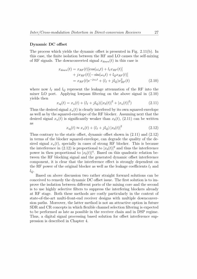
Inter/Cross-modulation Distortion in Direct-conversion Receivers 27
Dynamic DC offset
The process which yields the dynamic offset is presented in Fig. 2.11(b). Inthis case, the finite isolation between the RF and LO causes the self-mixingof RF signals. The downconverted signal xdown(t) in this case is
xdown(t) = xRF (t)[cos(ωut) + lIxRF (t)]
+ jxRF (t)[− sin(ωut) + lQxRF (t)]
= xRF (t)e−jωut + (lI + jlQ)x
2RF (t) (2.10)
where now lI and lQ represent the leakage attenuation of the RF into themixer LO port. Applying lowpass filtering on the above signal in (2.10)yields then
xiq(t) = xu(t) + (lI + jlQ)(|xb(t)|2 + |xu(t)|2) (2.11)
Thus the desired signal xu(t) is clearly interfered by its own squared-envelopeas well as by the squared-envelope of the RF blocker. Assuming next that thedesired signal xu(t) is significantly weaker than xb(t), (2.11) can be writtenas
xiq(t) ≈ xu(t) + (lI + jlQ) |xb(t)|2 (2.12)
Thus contrary to the static offset, dynamic offset shown in (2.11) and (2.12)in terms of the blocker squared-envelope, can degrade the quality of the de-sired signal xu(t), specially in cases of strong RF blocker. This is becausethe interference in (2.12) is proportional to |xb(t)|2 and thus the interferencepower in then proportional to |xb(t)|4. Based on this quadratic relation be-tween the RF blocking signal and the generated dynamic offset interferencecomponent, it is clear that the interference effect is strongly dependent onthe RF power of the original blocker as well as the leakage coefficients lI andlQ.
Based on above discussion two rather straight forward solutions can beconceived to remedy the dynamic DC offset issue. The first solution is to im-prove the isolation between different ports of the mixing core and the secondis to use highly selective filters to suppress the interfering blockers alreadyat RF stage. Both these methods are costly particularly in the context ofstate-of-the-art multi-front-end receiver designs with multiple downconver-sion paths. Moreover, the latter method is not an attractive option in futureSDR and CR concepts in which flexible channel selection filtering is expectedto be performed as late as possible in the receiver chain and in DSP regime.Thus, a digital signal processing based solution for offset interference sup-pression is described in Chapter 4.

28 Nonlinear Distortion Effects in Direct-conversion Receivers

CHAPTER 3
DIGITAL CANCELLATION OFINTERMODULATION INDIRECT-CONVERSION
RECEIVERS
In this chapter, an adaptive IC method to suppress inter/cross-modulationdistortions caused by strong blocking signals on top of the desired signalbands as a result of LNA and last-stage amplification nonlinearities in DCRstructure is introduced. The basics of operation for this IC method are alsodiscussed. More detailed analysis and presentations on this method can befound in [P1] and [P4].
3.1 Basics of Interference Canceller Opera-tion
In Chapter 2, the essential inter/cross-modulation distortion models from thecomplex communications waveforms point of view were introduced. Here, wesimply assume that a collection of frequency channels is I/Q downconvertedas a whole and some of the downconverted strong signals create interferenceon top of the weaker signals as the result of odd- and even- nonlinearities inthe I/Q branches of the downconverter. Moreover, based on the discussion inSection 2.3.1, it is assumed that the LNA contributes to the interference pro-file only through odd-order cross-modulation terms, therefore the even-orderinter/cross-modulation terms stemming from LNA are ignored. The basiccompensation structure is presented in Fig. 3.1. The idea is to consider the

30 Digital Cancellation of Intermodulation in Direct-conversion Receivers
Figure 3.1: Proposed compensation structure. The upper branch capturesthe desired signal band and the lower branch generates an interference ref-erence. These two signals are then processed by an adaptive interferencecanceller to suppress the nonlinear distortion effects from the signal of inter-est
detection of the interesting signals on a channel-by-channel basis, such thatthe band-split filtering stage first separates the desired signal band, aroundω0, and all the other signals. These effective filtering functions are denotedby HI
D, HQD , H
IR and HQ
R with their corresponding impulse responses hID(n),
hQD(n), hIR(n) and h
QR(n), respectively. Here, “D” refers to “desired” and “R”
to “reference” signal branches and superscript I and Q signify whether thefilter belongs to I or Q branch. As the entire IC algorithm is implemented indigital domain discrete time notations are employed to describe the behaviorof the compensation algorithm. Notice also that the processing depicted inFig. 3.1 is carried out separately for the physical I and Q signal branches.
Filtering the nonlinear component output, the signals at the band-splittingfilters output and for I and Q branches reads
yD,I(n) = hID(n) ∗ yI(n) ≈ xD,I(n) + nD,I(n) (3.1)
yR,I(n) = hIR(n) ∗ yI(n) ≈ xR,I(n) + nR,I(n)
yD,Q(n) = hQD(n) ∗ yQ(n) ≈ xD,Q(n) + nD,Q(n)
yR,Q(n) = hQR(n) ∗ yQ(n) ≈ xR,Q(n) + nR,Q(n)
Here yI(n) and yQ(n) are the outputs of the nonlinear elements in I and Qbranches of the I/Q downconverter, respectively. Moreover, in (3.1), xD,I(n),xD,Q(n), xR,I(n) and xR,Q(n) are the I/Q components of the original signalsin the desired band and the reference bands, respectively. The spurious fre-quencies stemming from nonlinear component in the desired band and thereference band are denoted by nD,I(n), nD,Q(n), nR,I(n) and nR,Q(n), respec-tively. The idea in this structure is to regenerate the distorting inter/cross-modulation components nD,I(n) and nD,Q(n) by feeding the reference branchsignals yR,I(n) and yR,Q(n) into a model of the nonlinear process (Fig.3.1).
Basics of Interference Canceller Operation 31
Naturally, the nonlinear model generates the interfering as well as non-interfering inter/cross-modulation terms, therefore a band-limiter filter isrequired to isolate the interfering inter/cross-modulation terms, i.e. nD,I(n)and nD,Q(n) (Fig.3.1). After the generation of these terms an adaptive filter-ing stage is applied to ”scale” the reproduced frequency components prop-erly before being subtracted from the desired signal observation. The adap-tive filter coefficients vectors, wI(n) = [w0,I(n), w1,I(n), . . . , wL−1,I(n)]
T andwQ(n) = [w0,Q(n), w1,Q(n), . . . , wL−1,Q(n)]
T can be adjusted, e.g., to mini-mize the power of the compensator output using the well-known least-mean-square (LMS) algorithm [64] as follows
wI(n+ 1) = wI(n) + µnD,I(n)xD,I(n) (3.2)
= wI(n) + µnD,I(n)[yD,I(n)−wT
I (n)nD,I(n)]
= wI(n) + µnD,I(n)[xD,I(n) + nD,I(n)−wT
I (n)nD,I(n)]
and
wQ(n+ 1) = wQ(n) + µnD,Q(n)xD,Q(n) (3.3)
= wQ(n) + µnD,Q(n)[yD,Q(n)−wT
Q(n)nD,Q(n)]
= wQ(n) + µnD,Q(n)[xD,Q(n) + nD,Q(n)−wT
Q(n)nD,Q(n)]
where outputs of the interference canceller in I and Q branches are xD,I(n)and xD,Q(n). Moreover, the adaptive filter input vectors for I and Q branchesare nD,I(n) = [nD,I(n), nD,I(n − 1), . . . , nD,I(n − L + 1)]T and nD,Q(n) =[nD,Q(n), nD,Q(n − 1), . . . , nD,Q(n − L + 1)]T , respectively. Also, µ is thestep-size for the coefficients update of the LMS algorithm. Note that, in casethe nonlinear device doesn’t exhibit any memory here the adaptive filters inI and Q branches are reduced to one-tap. In practical implementation, theeffective processing of second-order, third-order, etc. interference can be car-ried out individually, by having parallel reference signal branches (referencenonlinearity and adaptive filter stage) for each order of interest i.e. separatenD(n) is generated for different orders of nonlinearity. In this way, the neededreference polynomials are simply quadratic, cubic, etc., operators, in the sim-plest case, and the corresponding adaptive filters process each order effectsseparately. Thus, in general, it should be noted that no detailed model of thenonlinear physical front-end is necessarily needed. The reference nonlinearitysection simply regenerates the interfering frequency components which arethen further modified by the online adaptive filter stage, controlling the ac-tual interference cancellation process. In general, by adjusting the band-splitfiltering stage separating desired signal from the rest of the spectrum, thismethod is applicable independently of the position of the desired signal.
To establish a concrete understanding on the operation of this IC algo-rithm, two examples from the operation of this algorithm to compensate the
32 Digital Cancellation of Intermodulation in Direct-conversion Receivers
effects of a nonlinear LNA and nonlinearity in I/Q branches of a downcon-verter are presented here.
3.1.1 Case A: LNA Nonlinearity
In the first case, let’s assume an LNA with a third-order polynomial charac-teristics as follows
yRF (t) = a1xRF (t) + a2x2RF (t) + a3x
3RF (t) (3.4)
where a1, a2 and a3 are real-valued coefficients. The signal model for the LNAinput is the three-signal model, which is used in previous chapter, includinga desired signal and two blockers as follows
xRF (t) = A0(t) cos(ω0t+ ϕ0(t)) + A1(t) cos(ω1t+ ϕ1(t))
+ A2(t) cos(ω2t+ ϕ2(t)) (3.5)
According to the detailed derivations for the inter/cross-modulations of suchsignal model which are presented in Appendix A.1, yRF (t) includes hosts ofspurious components resulting from second- and third-order nonlinearities.On the other hand, it is already established in Chapter 2 that the dominantinterference components caused by LNA on top of the desired signal aremainly the third(odd)-order cross-modulations of the blockers. Here, we as-
sume 2ω1−ω2 ≈ ω0 which means cross-modulation term a33A2
1(t)A2(t)
4cos((2ω1−
ω2)t + 2ϕ1(t) − ϕ2(t)) is the interfering term. Let’s also assume that thenonlinearity-generated spurious components outside the desired band are sig-nificantly weaker compare to the blockers. Considering the above assump-tions, the output of the LNA follows
yRF (t) ≈ a1A0(t) cos(ω0t+ ϕ0(t)) (3.6)
+ a33A2
1(t)A2(t)
4cos((2ω1 − ω2)t+ 2ϕ1(t)− ϕ2(t))
+ a1A1(t) cos(ω1t+ ϕ1(t)) + a1A2(t) cos(ω2t+ ϕ2(t))
The I/Q downconverted version of the LNA output, y(t), then reads
y(t) ≈ a1A0(t)ej(ω0t+ϕ0(t)) + a3
3A21(t)A2(t)
4ej((2ω1−ω2)t+2ϕ1(t)−ϕ2(t)) (3.7)
+ a1A1(t)ej(ω1t+ϕ1(t)) + a1A2(t)e
j(ω2t+ϕ2(t))
Note that, the I/Q branches of the downconverter are assumed to be linearin this example. The discrete-time I/Q components of y(t), i.e. yI(n) and

Basics of Interference Canceller Operation 33
yQ(n), are written as follows
yI(n) = a1A0(nTs) cos (ω0nTs + ϕ0(nTs)) (3.8)
+ a33A2
1(nTs)A2(nTs)
4cos ((2ω1 − ω2)nTs + 2ϕ1(nTs)− ϕ2(nTs))
+ a1A1(nTs) cos (ω1nTs + ϕ1(nTs)) + a1A2(nTs) cos (ω2nTs + ϕ2(nTs))
yQ(n) = a1A0(nTs) sin (ω0nTs + ϕ0(nTs))
+ a33A2
1(nTs)A2(nTs)
4sin ((2ω1 − ω2)nTs + 2ϕ1(nTs)− ϕ2(nTs))
+ a1A1(nTs) sin (ω1nTs + ϕ1(nTs)) + a1A2(nTs) sin (ω2nTs + ϕ2(nTs))
Here, Ts is the sampling time. Afterward, the signals yI(n) and yQ(n) are splitinto desired and reference bands. The signals in the desired and referencebranches of IC algorithm reads from (3.1)
yD,I(n) ≈ xD,I(n) + nD,I(n) (3.9)
= a1A0(nTs) cos (ω0nTs + ϕ0(nTs))
+ a33A2
1(nTs)A2(nTs)
4cos ((2ω1 − ω2)nTs + 2ϕ1(nTs)− ϕ2(nTs))
yD,Q(n) ≈ xD,Q(n) + nD,Q(n)
= a1A0(nTs) sin (ω0nTs + ϕ0(nTs))
+ a33A2
1(nTs)A2(nTs)
4sin ((2ω1 − ω2)nTs + 2ϕ1(nTs)− ϕ2(nTs))
yR,I(n) ≈ xR,I(n) + nR,I(n) ≈ xR,I(n)
= a1A1(nTs) cos (ω1nTs + ϕ1(nTs)) + a1A2(nTs) cos (ω2nTs + ϕ2(nTs))
yR,Q(n) ≈ xR,Q(n) + nR,Q(n) ≈ xR,Q(n)
= a1A1(nTs) sin (ω1nTs + ϕ1(nTs)) + a1A2(nTs) sin (ω2nTs + ϕ2(nTs))
One should note that the spurious components on the reference branches areassumed to be negligible comparing to the blockers, hence E[|nR,I(n)|2] ≪E[|xR,I(n)|2] and E[|nR,Q(n)|2] ≪ E[|xR,Q(n)|2]. In order to regenerate theinterfering component on top of the desired signal the isolated blockers inyR,I(n) and yR,Q(n) are passed through a simple cubic term. The output ofthe cubic element, then, reads
y3R,I(n) = (3.10)
3a31A21(nTs)A2(nTs)
4cos ((2ω1 − ω2)nTs + 2ϕ1(nTs)− ϕ2(nTs)) + Re[Ξ
IM/CM3 ]
y3R,Q(n) =
3a31A21(nTs)A2(nTs)
4sin ((2ω1 − ω2)nTs + 2ϕ1(nTs)− ϕ2(nTs)) + Im[Ξ
IM/CM3 ]

34 Digital Cancellation of Intermodulation in Direct-conversion Receivers
where all the third-order complex inter/cross-modulation terms outside the
desired band, i.e. around ω0, are denoted by ΞIM/CM3 . The outputs of the
band limiting filters in I and Q branches, nD,I(n) and nD,Q(n), then read
nD,I(n) ≈3a31A
21(nTs)A2(nTs)
4cos ((2ω1 − ω2)nTs + 2ϕ1(nTs)− ϕ2(nTs))
(3.11)
nD,Q(n) ≈3a31A
21(nTs)A2(nTs)
4sin ((2ω1 − ω2)nTs + 2ϕ1(nTs)− ϕ2(nTs))
Comparing (3.9) and (3.11), one can notice that the difference between theactual interfering terms on top of the real and imaginary parts of the desiredsignal, i.e. nD,I(n) and nD,Q(n), and the corresponding regenerated versionsof these terms at the band-limiting filters output, i.e. nD,I(n) and nD,Q(n),is a scaling factor a3/a
31. This coefficient then can be estimated using the
adaptive algorithm presented in (3.2) and (3.3) and finally the scaled versionof the nD,I(n) and nD,Q(n) are subtracted from the desired branch which inturn cancel out the interfering terms generated by LNA.
3.1.2 Case B: Nonlinearity in I and Q Branches of theDownconverter
The second case studies the operation of IC algorithm in presence of nonlinearelements in the I/Q branches of an I/Q downconverter. The three-signalmodel is again used here for demonstration purpose. The complex basebandversion of the downconverted signal before the nonlinear elements reads
x(t) = A0(t)ej(ω0t+ϕ0(t)) + A1(t)e
j(ω1t+ϕ1(t)) + A2(t)ej(ω2t+ϕ2(t)) (3.12)
In this example we assumed third-order polynomial characteristics with equalcoefficients for both I and Q branches. Therefore, the input/output relationsof the I and Q nonlinear elements are defined as follow
yI(t) = b1xI(t) + b2x2I(t) + b3x
3I(t) (3.13)
yQ(t) = b1xQ(t) + b2x2Q(t) + b3x
3Q(t)
where b1, b2 and b3 are real-valued coefficients. Furthermore, and for math-ematical tractability, we assume that ω1 = ω0
3and ω2 = 2ω0
3which in turn
means the second-order cross-modulation term of the blockers at ω1 + ω2
and the third-order cross-modulation term at 2ω2 − ω1 interfere with thedesired signal at ω0. With the above assumptions, the signal at the I/Q

Basics of Interference Canceller Operation 35
downconverter output reads
y(t) ≈ b1A0(t)ej(ω0t+ϕ0(t)) (3.14)
+ b2(1− j)A1(t)A2(t) cos ((ω1 + ω2)t+ ϕ1(t) + ϕ2(t))
+ b33A2
2(t)A1(t)
4ej((2ω2−ω1)t+2ϕ2(t)−ϕ1(t))
+ b1A1(t)ej(ω1t+ϕ1(t)) + b1A2(t)e
j(ω2t+ϕ2(t))
The discrete-time I/Q components of y(t) , i.e. yI(n) and yQ(n), are writtenas follows
yI(n) = b1A0(nTs) cos (ω0nTs + ϕ0(nTs)) (3.15)
+ b2A1(nTs)A2(nTs) cos ((ω1 + ω2)nTs + ϕ1(nTs) + ϕ2(nTs))
+ b33A2
2(nTs)A1(nTs)
4cos ((2ω2 − ω1)nTs + 2ϕ2(nTs)− ϕ1(nTs))
+ b1A1(nTs) cos (ω1nTs + ϕ1(nTs)) + b1A2(nTs) cos (ω2nTs + ϕ2(nTs))
yQ(n) = b1A0(nTs) sin (ω0nTs + ϕ0(nTs))
− b2A1(nTs)A2(nTs) cos ((ω1 + ω2)nTs + ϕ1(nTs) + ϕ2(nTs))
+ b33A2
2(nTs)A1(nTs)
4sin ((2ω2 − ω1)nTs + 2ϕ2(nTs)− ϕ1(nTs))
+ b1A1(nTs) sin (ω1nTs + ϕ1(nTs)) + b1A2(nTs) sin (ω2nTs + ϕ2(nTs))
Afterward, the signals yI(n) and yQ(n) are split into desired and referencebands. The signals in the desired and reference branches of IC, from (3.1),reads
yD,I(n) ≈ xD,I(n) + nD,I(n) (3.16)
= b1A0(nTs) cos (ω0nTs + ϕ0(nTs))
+ b2A1(nTs)A2(nTs) cos ((ω1 + ω2)nTs + ϕ1(nTs) + ϕ2(nTs))
+ b33A2
2(nTs)A1(nTs)
4cos ((2ω2 − ω1)nTs + 2ϕ2(t)− ϕ1(nTs))
yD,Q(n) ≈ xD,Q(n) + nD,Q(n)
= b1A0(nTs) sin (ω0nTs + ϕ0(nTs))
− b2A1(nTs)A2(nTs) cos ((ω1 + ω2)nTs + ϕ1(nTs) + ϕ2(nTs))
+ b33A2
2(nTs)A1(nTs)
4sin ((2ω2 − ω1)nTs + 2ϕ2(nTs)− ϕ1(nTs))
yR,I(n) ≈ xR,I(n) + nR,I(n) ≈ xR,I(n)
= b1A1(nTs) cos (ω1nTs + ϕ1(nTs)) + b1A2(nTs) cos (ω2nTs + ϕ2(nTs))
yR,Q(n) ≈ xR,Q(n) + nR,Q(n) ≈ xR,Q(n)
= b1A1(nTs) sin (ω1nTs + ϕ1(nTs)) + b1A2(nTs) sin (ω2nTs + ϕ2(nTs))

36 Digital Cancellation of Intermodulation in Direct-conversion Receivers
Again, similar to LNA case it is assumed that the spurious components onthe reference branches are negligible comparing to the blockers. In orderto regenerate the second-order interfering component on top of the desiredsignal the isolated blockers in yR,I(n) and yR,Q(n) are passed through simplequadratic elements. The outputs of the second-order elements, then, read
y2R,I(n) = (3.17)
b21A1(nTs)A2(nTs) cos ((ω1 + ω2)nTs + ϕ1(nTs) + ϕ2(nTs)) + Re[ΞIM/CM2 ]
y2R,Q(n) =
b21A1(nTs)A2(nTs) cos ((ω1 + ω2)nTs + ϕ1(nTs) + ϕ2(nTs)) + Im[ΞIM/CM2 ]
where all the complex second-order inter/cross-modulation terms outside the
desired band, i.e. around ω0, are denoted by ΞIM/CM2 . The output of the
band-limiting filters for the quadratic elements in I and Q branches, i.e.
n(2)D,I(n) and n
(2)D,Q(n) from Fig. 3.2, reads
n(2)D,I(n) = b21A1(nTs)A2(nTs) cos ((ω1 + ω2)nTs + ϕ1(nTs) + ϕ2(nTs))
(3.18)
n(2)D,Q(n) = b21A1(nTs)A2(nTs) cos ((ω1 + ω2)nTs + ϕ1(nTs) + ϕ2(nTs))
It is clear then that the second-order interference in the desired branch of theIC algorithm in (3.16) is the scaled version of the regenerated interference
which is presented in (3.18). Thus, proper scaling of the n(2)D,I(n) and n
(2)D,Q(n)
using the mentioned adaptive algorithm and subtracting the result eliminatesthe second-order interference from the desired signal band.
To suppress the third-order interference separate paths with cubic ele-ments are employed in the IC algorithm reference paths. The cubic termoutputs, in turn, are written as
y3R,I(n) = (3.19)
3b31A22(nTs)A1(nTs)
4cos ((2ω2 − ω1)nTs + 2ϕ2(nTs)− ϕ1(nTs)) + Re[Ξ
IM/CM3 ]
y3R,Q(n) =
3b31A22(nTs)A1(nTs)
4sin ((2ω2 − ω1)nTs + 2ϕ2(nTs)− ϕ1(nTs)) + Im[Ξ
IM/CM3 ]
The outputs of the band limiting filters in I and Q branches, n(3)D,I(n) and

Basics of Interference Canceller Operation 37
n(3)D,Q(n) from Fig. 3.2, read
n(3)D,I(n) =
3b31A22(nTs)A1(nTs)
4cos ((2ω2 − ω1)nTs + 2ϕ2(nTs)− ϕ1(nTs))
(3.20)
n(3)D,Q(n) =
3b31A22(nTs)A1(nTs)
4sin ((2ω2 − ω1)nTs + 2ϕ2(nTs)− ϕ1(nTs))
Here, similar to second-order case, the third-order interfering terms are re-generated up to a scaling factor. The scaling factor is estimated using theLMS adaptive algorithm mentioned above and the final scaled version of theregenerated interfering terms are subtracted from the desired signal branchesof the IC algorithm in both I and Q branches.
In the above examples two following assumptions are used for the opera-tion of IC algorithm
• E[|nR(n)|2] ≪ E[|xR(n)|2] which means the power of the blockers aresignificantly higher than all the inter/cross-modulations that fall in thereference branches of IC algorithm.
• nD(n) is dominated by inter/cross-modulations of the blockers.
Hereafter, we justify the validity of these two assumptions in practical re-ceivers again invoking on the three-signal model and I/Q nonlinearity case.Needless to say that the same arguments can be extended for the nonlin-ear LNA case. According to two-blocker scenario the spurious frequenciesgenerated by third-order nonlinearity that can hit the reference band are asfollows (Table A.4 in the Appendix)
Self-distortion components (e.g. b3(1+g3)2
(3A3
1(t)
4+
3A22(t)A1(t)
2+
3A20(t)A1(t)
2)ej(ω1t+ϕ1(t))) These components hit the blockers frequencies.
However, as the nonlinear component is assumed to be mild, i.e. b3 ≪b1, then these interfering components are orders of magnitude weakerthan the blockers themselves and can be neglected.
Cross-modulations of two blockers (e.g.b3(1+g3)
2(3A2
1(t)A2(t)
4ej((2ω1−ω2)t+2ϕ1(t)−ϕ2(t)))) Again with the mild linear-
ity assumption in mind, these components can be ignored as they aresignificantly weaker comparing to the power of the original blockers.
Cross-modulations of the desired signal and one blocker (e.g.b3(1+g3)
2
3A21(t)A0(t)
4ej((2ω1−ω0)t+2ϕ1(t)−ϕ0(t))) The envelopes of these compo-
nents are proportional to the desired signal envelope and as the desiredsignal is significantly weaker than the blockers these components areinsignificant.

38 Digital Cancellation of Intermodulation in Direct-conversion Receivers
Cross-modulations of the desired signal and both blockers (e.gb3(1+g3)
26A0(t)A1(t)A2(t)
4e(j(ω1−ω2+ω0)t+ϕ1(t)−ϕ2(t)+ϕ0(t))) The envelopes of these
components are also proportional to the desired signal envelope and asthe desired signal is significantly weaker than the blockers these com-ponents are insignificant.
As for the second-order nonlinearity the terms that can hit the referenceband are listed below (Table A.4 in the Appendix)
IMD term from interaction of the desired signal and one blocker (e.g.b2(1+jg2)A1(t)A0(t) cos((ω1−ω0)t+ϕ1(t)−ϕ0(t))) The nonlinear com-ponent assumed to be mild b2 ≪ b1. Moreover, the envelopes of thesecomponents are proportional to the weak desired signal envelope. All inall, these components can be ignored in comparison to strong blockersin reference band.
IMD term from interaction of the two blockers (e.g.b2(1− jg2)A1(t)A2(t) cos((ω1+ ω2)t+ϕ1(t)+ϕ2(t))) Again, these com-ponents can be ignored with the mild nonlinearity assumption b2 ≪ b1.
Following the above discussion, it is possible to conclude that in practicalimplementations the assumption E[|nR(n)|2] ≪ E[|xR(n)|2] is valid. Never-theless, with the mild nonlinearity and weak desired signal assumption theresults of above examples can be extended to the higher order nonlinear-ity and larger number of blockers. To examine the second assumption, i.e.nD(n) should be only generated by the blockers captured in the referencebranch, we again refer to the example which is presented in the AppendixSection A.2. A closer look at the derivations for second- and third-orderspurious frequencies (Tables A.4 and A.3 in the Appendix) shows that allthe components interfering with desired band can be ignored comparing tothe blockers second- and third-order cross-modulations, considering the weakdesired signal and mild nonlinearity assumptions. This, in turn, means thedominant interference on top of the desired signal band is generated by theblockers which are captured in the reference band.
3.2 Computer Simulation and Laboratory Mea-surement Examples
To illustrate the basic idea of the proposed compensation principle, purelycomputer simulation based results are presented here first. In this experi-ment, the desired signal is QPSK modulated signal located at f0 =103 MHzRF carrier with roughly 1-MHz RF bandwidth. The blocker in this case is anamplitude modulated (AM) at f1 =98.95 MHz RF center frequency with 100

Computer Simulation and Laboratory Measurement Examples 39
Figure 3.2: Detailed representation of the IC algorithm designed for com-pensation of second- and third-order cross-modulation interfering terms.
kHz modulating tone and 20% modulation index and the power differencebetween the blocker and the desired signal is set to 40 dB. The LO frequencyin this experiment is set to 100 MHz and third-order nonlinearity is imple-mented in the I/Q downconversion process. After the downconversion the
desired signal and the blocker are located at f0 =3MHz and f1 = −1.05 MHz.Moreover, as the result of third-order nonlinearity process the AM blockergenerates harmonics at 2.85, 3.15 and 3.45 MHz and intermodulation termsat 2.95, 3.05, 3.25 and 3.35 MHz which all fall on top of the desired signalat IF. The obtained results are illustrated in Fig. 3.3, in terms of the down-converted complex signal spectrum as well as demodulated desired signal atsymbol rate without and with digital compensation. The adaptation of theIC coefficients are implemented using the LMS algorithm which is describedin previous section. Without compensation, the demodulated desired signalis useless as such. However, by using the proposed compensator, virtuallyall the essential interference can be suppressed, resulting in close-to perfectQPSK signal constellations as can be seen in Fig. 3.3.
Next results obtained using actual laboratory signal measurements arereported. For illustration, exactly the same RF waveform setups as in Sub-section 2.3.1 is used. The desired signal is QPSK modulated with 800 kHzsymbol rate and located at 103 MHz RF carrier. The pulse-shape is a raised-cosine pulse with 30% roll-off, yielding roughly 1 MHz RF bandwidth. Noticethat “down-scaled” RF frequencies in the order of 100 MHz are used simplyto facilitate the measurement system implementation (cabling requirements,etc.) and do not play any other role here. I/Q downconversion with 100 MHzLO signal(s) translates the desired signal to 3 MHz IF. The strong blockerin this experiment is a sinusoidal at 98.6 MHz RF frequency. This results insecond-order harmonic distortion component on top of the desired signal at2.8 MHz (after I/Q downconversion). After I/Q downconverting the signals
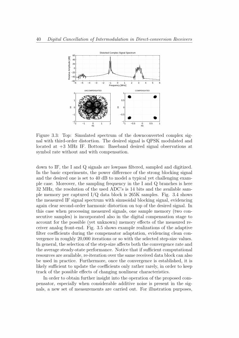
40 Digital Cancellation of Intermodulation in Direct-conversion Receivers
−6 −5 −4 −3 −2 −1 0 1 2 3 4 5 6−60
−40
−20
0
20
40
60
Frequency [MHz]
Distorted Complex Signal Spectrum
Rel
ativ
e A
mpl
itude
[dB
]
−2 −1 0 1 2−2
−1
0
1
2UNCOMPENSATED
RE
IM
−1 −0.5 0 0.5 1−1
−0.5
0
0.5
1COMPENSATED
RE
IM
Figure 3.3: Top: Simulated spectrum of the downconverted complex sig-nal with third-order distortion. The desired signal is QPSK modulated andlocated at +3 MHz IF. Bottom: Baseband desired signal observations atsymbol rate without and with compensation.
down to IF, the I and Q signals are lowpass filtered, sampled and digitized.In the basic experiments, the power difference of the strong blocking signaland the desired one is set to 40 dB to model a typical yet challenging exam-ple case. Moreover, the sampling frequency in the I and Q branches is here32 MHz, the resolution of the used ADC’s is 14 bits and the available sam-ple memory per captured I/Q data block is 265K samples. Fig. 3.4 showsthe measured IF signal spectrum with sinusoidal blocking signal, evidencingagain clear second-order harmonic distortion on top of the desired signal. Inthis case when processing measured signals, one sample memory (two con-secutive samples) is incorporated also in the digital compensation stage toaccount for the possible (yet unknown) memory effects of the measured re-ceiver analog front-end. Fig. 3.5 shows example realizations of the adaptivefilter coefficients during the compensator adaptation, evidencing clean con-vergence in roughly 20,000 iterations or so with the selected step-size values.In general, the selection of the step-size affects both the convergence rate andthe average steady-state performance. Notice that if sufficient computationalresources are available, re-iteration over the same received data block can alsobe used in practice. Furthermore, once the convergence is established, it islikely sufficient to update the coefficients only rather rarely, in order to keeptrack of the possible effects of changing nonlinear characteristics.
In order to obtain further insight into the operation of the proposed com-pensator, especially when considerable additive noise is present in the sig-nals, a new set of measurements are carried out. For illustration purposes,
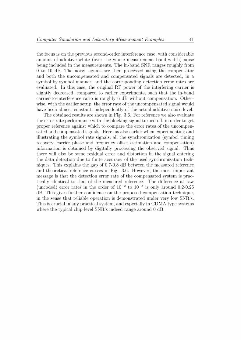
Computer Simulation and Laboratory Measurement Examples 41
the focus is on the previous second-order interference case, with considerableamount of additive white (over the whole measurement band-width) noisebeing included in the measurements. The in-band SNR ranges roughly from0 to 10 dB. The noisy signals are then processed using the compensatorand both the uncompensated and compensated signals are detected, in asymbol-by-symbol manner, and the corresponding detection error rates areevaluated. In this case, the original RF power of the interfering carrier isslightly decreased, compared to earlier experiments, such that the in-bandcarrier-to-interference ratio is roughly 6 dB without compensation. Other-wise, with the earlier setup, the error rate of the uncompensated signal wouldhave been almost constant, independently of the actual additive noise level.
The obtained results are shown in Fig. 3.6. For reference we also evaluatethe error rate performance with the blocking signal turned off, in order to getproper reference against which to compare the error rates of the uncompen-sated and compensated signals. Here, as also earlier when experimenting andillustrating the symbol rate signals, all the synchronization (symbol timingrecovery, carrier phase and frequency offset estimation and compensation)information is obtained by digitally processing the observed signal. Thusthere will also be some residual error and distortion in the signal enteringthe data detection due to finite accuracy of the used synchronization tech-niques. This explains the gap of 0.7-0.8 dB between the measured referenceand theoretical reference curves in Fig. 3.6. However, the most importantmessage is that the detection error rate of the compensated system is prac-tically identical to that of the measured reference. The difference at raw(uncoded) error rates in the order of 10−2 to 10−3 is only around 0.2-0.25dB. This gives further confidence on the proposed compensation technique,in the sense that reliable operation is demonstrated under very low SNR’s.This is crucial in any practical system, and especially in CDMA type systemswhere the typical chip-level SNR’s indeed range around 0 dB.

42 Digital Cancellation of Intermodulation in Direct-conversion Receivers
−8 −7 −6 −5 −4 −3 −2 −1 0 1 2 3 4 5 6 7 8−40
−20
0
20
40
60
Spectrum of the Measured IF Signal, fIF
= 3MHz, fSYM
= 800kHz
Frequency [MHz]
Rel
ativ
e A
mpl
itude
[dB
]
−1 −0.5 0 0.5 1−1
−0.5
0
0.5
1UNCOMPENSATED
RE
IM
−1 0 1
−1
0
1
COMPENSATED
RE
IM
Figure 3.4: Upper part: Measured IF signal spectrum with sinusoidal blocker.The desired signal is QPSK modulated and located at +3 MHz IF. Lowerpart: Baseband desired signal observations at symbol rate without and withcompensation.
0 2 4 6 8 10
x 104
0
0.5
1
1.5
2IC Coefficient, I(n)2
Iteration #
AB
S
0 2 4 6 8 10
x 104
0
0.2
0.4
0.6
0.8
1IC Coefficient, I(n)´ I(n−1)
Iteration #
AB
S
0 2 4 6 8 10
x 104
0
0.5
1
1.5
2IC Coefficient, Q(n)2
Iteration #
AB
S
0 2 4 6 8 10
x 104
0
0.2
0.4
0.6
0.8
1IC Coefficient, Q(n)´ Q(n−1)
Iteration #
AB
S
Figure 3.5: Example realization of the adaptive IC coefficients. Quadraticelements coefficients for I/Q branches of IC algorithm (top row) and memoryelements coefficients for I/Q branches of IC algorithm (bottom row).

Computer Simulation and Laboratory Measurement Examples 43
0 1 2 3 4 5 6 7 8 9 10 11
10−4
10−3
10−2
10−1
100
In−Band SNR [dB]
SE
R
QPSK Detection Error Rate vs. In−Band SNR
UncompensatedCompensatedMeasured Noise BoundTheoretical Noise Bound
Figure 3.6: Symbol error rate (SER) performance with measured signalsas a function of additive noise level. QPSK modulated desired signal andsinusoidal blocker. The in-band carrier-to-interference (C/I) ratio is around6 dB without compensation.

44 Digital Cancellation of Intermodulation in Direct-conversion Receivers

CHAPTER 4
DIGITAL MITIGATION OFDYNAMIC OFFSET IN DIVERSITY
RECEIVERS
4.1 Modeling Dynamic Offset in Diversity Re-ceiver
The mechanism resulting in dynamic DC-offset interference in DCR is alreadyexplained in Subsection 2.3.3. For convenience, we repeat the expression forthe downconverted desired signal including the dynamic DC-offset effect inthe following
xiq(t) = ζuxu(t) + |ζb|2 (lI + jlQ) |xb(t)|2 + xγ(t) (4.1)
In order to construct a more realistic model, the effects of additive whiteGaussian noise (AWGN) as well as the desired signal and blocker channelgains are also included in (4.1) where xγ(t) is a zero-mean white Gaussiannoise. Also the relative complex channel gains of the desired signal and theblocker at ωu and ωb are represented by ζu and ζb, respectively. Hereafter, anovel method for mitigation of dynamic DC-offset interference in two-antennadiversity receiver systems is addressed. The proposed method is motivatedby high cost and rigidness of traditional approaches (see Subsection 2.3.3) indealing with dynamic DC-offset interference in the context of modern multi-antenna SDR/CR receivers. The choice of two receiver paths, without lossof generality, is to keep the discussion practically oriented and applicable inmobile devices, where the two-antenna receiver case is indeed feasible.
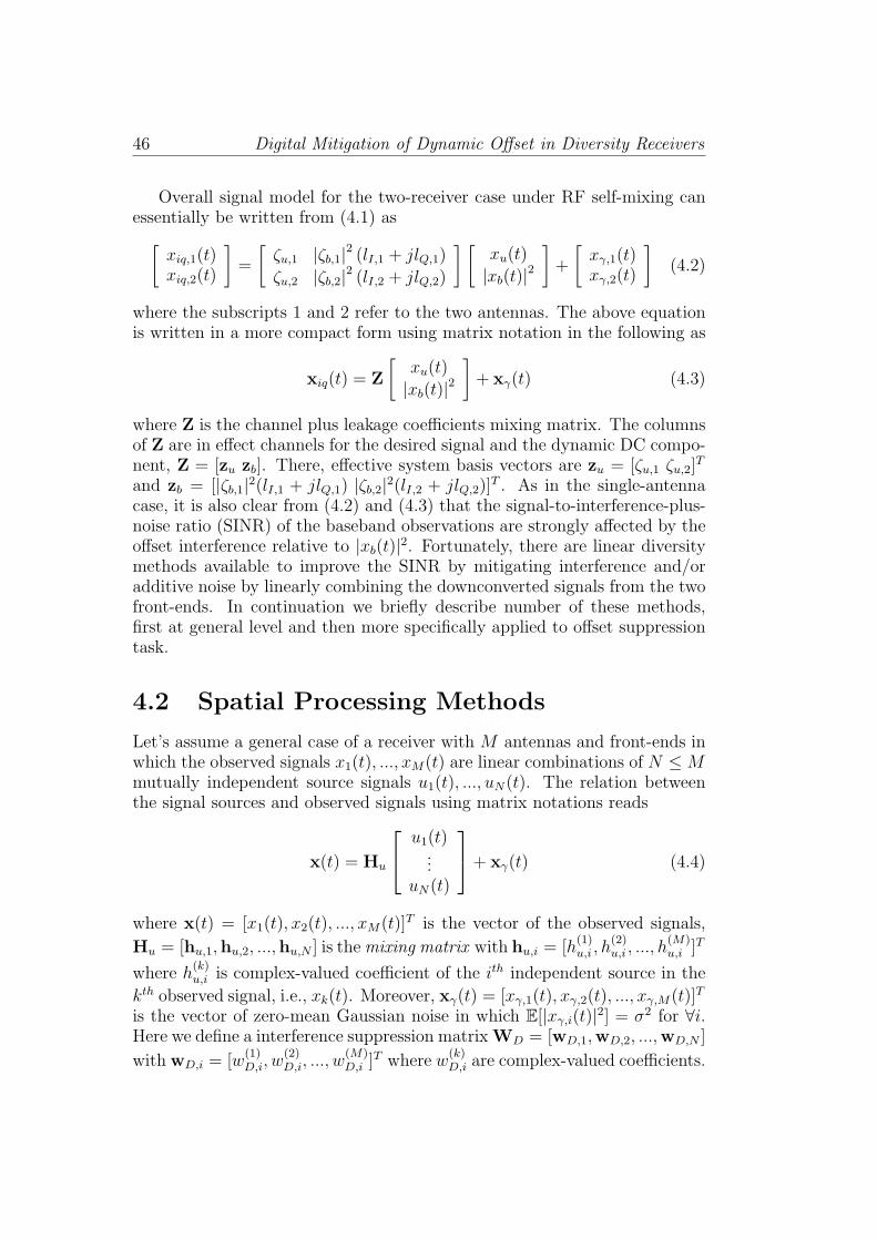
46 Digital Mitigation of Dynamic Offset in Diversity Receivers
Overall signal model for the two-receiver case under RF self-mixing canessentially be written from (4.1) as[
xiq,1(t)xiq,2(t)
]=
[ζu,1 |ζb,1|2 (lI,1 + jlQ,1)
ζu,2 |ζb,2|2 (lI,2 + jlQ,2)
] [xu(t)
|xb(t)|2]+
[xγ,1(t)xγ,2(t)
](4.2)
where the subscripts 1 and 2 refer to the two antennas. The above equationis written in a more compact form using matrix notation in the following as
xiq(t) = Z
[xu(t)
|xb(t)|2]+ xγ(t) (4.3)
where Z is the channel plus leakage coefficients mixing matrix. The columnsof Z are in effect channels for the desired signal and the dynamic DC compo-nent, Z = [zu zb]. There, effective system basis vectors are zu = [ζu,1 ζu,2]
T
and zb = [|ζb,1|2(lI,1 + jlQ,1) |ζb,2|2(lI,2 + jlQ,2)]T . As in the single-antenna
case, it is also clear from (4.2) and (4.3) that the signal-to-interference-plus-noise ratio (SINR) of the baseband observations are strongly affected by theoffset interference relative to |xb(t)|2. Fortunately, there are linear diversitymethods available to improve the SINR by mitigating interference and/oradditive noise by linearly combining the downconverted signals from the twofront-ends. In continuation we briefly describe number of these methods,first at general level and then more specifically applied to offset suppressiontask.
4.2 Spatial Processing Methods
Let’s assume a general case of a receiver with M antennas and front-ends inwhich the observed signals x1(t), ..., xM(t) are linear combinations of N ≤Mmutually independent source signals u1(t), ..., uN(t). The relation betweenthe signal sources and observed signals using matrix notations reads
x(t) = Hu
u1(t)...
uN(t)
+ xγ(t) (4.4)
where x(t) = [x1(t), x2(t), ..., xM(t)]T is the vector of the observed signals,
Hu = [hu,1,hu,2, ...,hu,N ] is themixing matrix with hu,i = [h(1)u,i , h
(2)u,i , ..., h
(M)u,i ]
T
where h(k)u,i is complex-valued coefficient of the ith independent source in the
kth observed signal, i.e., xk(t). Moreover, xγ(t) = [xγ,1(t), xγ,2(t), ..., xγ,M(t)]T
is the vector of zero-mean Gaussian noise in which E[|xγ,i(t)|2] = σ2 for ∀i.Here we define a interference suppression matrixWD = [wD,1,wD,2, ...,wD,N ]
withwD,i = [w(1)D,i, w
(2)D,i, ..., w
(M)D,i ]
T where w(k)D,i are complex-valued coefficients.

Spatial Processing Methods 47
The improvement in S(I)NR is achieved by multiplying the observed signalvector x(t) by WH
D which yields
y(t) = WHDx(t) (4.5)
The vector at the output of the interference suppression matrix is y(t) =[y1(t), y2(t), ..., yN(t)]
T . The matrix WHD can be selected to invert the effect
of the mixing matrix, Hu, which means WHD = (HH
u Hu)−1HH
u given matrixHu is a full-rank matrix here. In literature this method is referred to as zeroforcing (ZF) [36,65]. The ZF method aims at removing the interference fromthe desired signal however it neglects the noise component. Therefore, ZFmethod can result in amplification of the independent noise element or noiseenhancement [36,65]. Another widely used linear spatial processing methodis motivated by match filter (MF) and is called maximum ratio combining(MRC) [66] also known in literature as matrix match filter (MMF) [36]. Thereceived signal vector in MRC is transformed using Hermitian of the mixingmatrix i.e. WH
D = HHu . Therefore, the linearly transformed vector y(t) reads,
y(t) = WHDHu
u1(t)...
uN(t)
+WHDxγ(t)
= HHu Hu
u1(t)...
uN(t)
+HHu xγ(t) (4.6)
Now MRC provides diversity for individual source signals against channelfading but it does not take the intermixing of the signals into account. Ineffect, only if Hu is orthogonal matrix, meaning that HH
u Hu is a diagonalmatrix, then the MRC also separates the source signals. In the general casewith non-orthogonal Hu, MRC is thus clearly suboptimal [66].
Another method which provides a compromise between MRC and ZFwhen both noise and interference are present is called SINR maximizinggeneralized Eigen-filter (M-GEF) [33, 54, 55]. This linear transform is thenatural reference in all performance evaluations as it yields the best SINRamong the linear transforms [54]. The transform for the source signal ui(t)is formally given by
yi(t) = wHD,ix(t) (4.7)
and the solution wD,i maximizing the SINR with ui(t) as the desired signalin yi(t) can be written as [33,54]
woptD,i = argmax
wD,i
wHD,iRuwD,i
wHD,i(R
′u + σ2I)wD,i
(4.8)

48 Digital Mitigation of Dynamic Offset in Diversity Receivers
in which
Ru = E[hu,ihHu,i]
R′u =
N∑j=1,j =i
E[hu,jhHu,j] (4.9)
In practice, wD,i can be calculated using the generalized Eigen-value filteringapproach [33,34,54], i.e. wD,i is equal to the Eigen-vector of the matrix (R′
u+σ2I)−1Ru corresponding to its largest Eigen-value. The largest Eigenvalueitself is the maximum SINR achievable by any linear filter [33, 34,54].
One important note on the discussed spatial processing methods so far isthat implementing any of the described methods requires the knowledge ofthe mixing matrix and the noise variance in the receiver side. In most practi-cal cases these values are not readily available for the receiver and needs to beestimated by transmitting extra symbols as training sequences. Therefore,devising a blind method to yield maximum SINR without the knowledge ofthe mixing matrix and noise power levels, although computationally moredemanding, eliminates the need for transmission of these extra symbols. Inthis context one blind method that provides powerful tools and algorithms isindependent component analysis (ICA) [67,68]. In the following section firstwe argue that the dynamic DC-offset issue in two-front-end receiver context,as it is formulated in (4.2), should be viewed as the special case of (4.4)and therefore implementing the spatial processing methods presented abovemitigate the dynamic DC-offset component to various extends. Thereafter,the application of ICA-based algorithms in this context, which is publishedin [P3], is introduced and finally, the performance of widely-implementedICA-based algorithm against the mentioned spatial processing methods aredemonstrated through the results which are obtained from computer simu-lation experiments [P3].
4.2.1 Dynamic Offset Suppression Using ICA
In its basic form, ICA can recover multiple statistically independent sourcesignals, up to scale and permutation by just observing linear mixtures ofthem [67, 68] similar to the one presented in (4.4). Although, the completeseparation of the interfering sources and desired signal in a noisy environmentis not theoretically possible [33,55], Nevertheless, the SINR provided by ICA,as such, is extremely close to the maximum achievable SINR by any linearmethod [33]. Thus in the context of diversity receivers, ICA can be consideredas a practical method of joint interference rejection and diversity combining.
The model (4.3) fits to the general instantaneous mixing model which isrequired by ICA, i.e. two formal statistically independent source signals xu(t)and |xb(t)|2 are linearly mixed and two (or more) separate observation from

Spatial Processing Methods 49
Figure 4.1: A conceptual presentation of a receiver with two front-ends im-plementing ICA algorithm to mitigate the dynamic DC-offset.
their mixtures are available to the receiver. Furthermore, assuming differentchannels and/or different leakage coefficients for the different receivers, themodels in (4.2) and (4.3) are always identifiable. The operation principle ofthe ICA algorithm in mitigating dynamic DC-offset in two-front-end receiveris depicted in Fig. 4.1. The ICA algorithm in dynamic DC-offset mitigationapplication maximizes the SINR both for desired signal and for the offsetcomponent at its output ports. However, in this particular application thedesired signal is the output we are interested in and the DC-offset is dis-carded. To assess the obtainable offset interference rejection capability ofthe ICA-based approach, a series of computer simulation results is providedhere. A similar two-receiver case as in the previous section is assumed. Inthe first simulation case the desired signal and the blocker modulations areQPSK and for the second simulation case the modulations for both desiredsignal and blocker are 16QAM. In the simulation setup, channel coefficientsζu,1, ζu,2, ζb,1 and ζb,2 are drawn randomly from the complex Gaussian dis-tribution with zero mean and variance of one. The additive noise sequences(xγ,1(t) and xγ,2(t)) are white Gaussian noise with given power levels definedin the Table 4.1, depending on the desired signal modulation type. Eachexperiment consists of receiving the two receivers’ signals for 50,000 symbolintervals, over which the ICA is then applied for mitigating the offset inter-ference. The practical ICA algorithm used here is the equivariant adaptivesource identification (EASI) algorithm [68]. In this algorithm the interferencesuppression matrix, WH
EASI , is iteratively updated according to the following

50 Digital Mitigation of Dynamic Offset in Diversity Receivers
rule
WHEASI(t+ 1) = WH
EASI(t)− µEASIM(t)y(t)WHEASI(t) (4.10)
in which µEASI is a scalar step size and the update matrix M(t) is definedas
M(t) = y(t)yH(t)− I+ f[y(t)]yH(t)− y(t)f[y(t)]H (4.11)
Here y(t) = WHEASI(t)xiq(t), I denotes identity matrix and f[.] is an arbitrary
nonlinear function. In these experiments f[.] is a simple third-order nonlinear-ity and adaptation step-size corresponding to convergence in the stated blocklength of 50,000 symbol intervals. The average output SINR is calculated forcomparing the performance of the ICA-based processing against M-GEF ref-erence (forming a theoretical bound for any linear interference cancellationmethod). In addition, assuming known channel state, also ZF and MRC arealso implemented for comparison, in which only either the interference (ZF)or additive noise (MRC) is conceptually taken into account. The averageSINR performances are obtained by averaging over 1000 different realizationof channel coefficients. The RF-LO leakage coefficients are in the order of-50 dB to -60 dB, which represent state-of-the-art.
The simulation parameters are summarized in Table 4.1. The obtainedoutput SINR results as a function of the in-band signal-to-interference ratio(SIR) before compensation, for the case 1 and 2 are presented in Fig. 4.2 andfig. 4.3, respectively. The interference free curve shows the average outputSINR in case that the dynamic offset interference could be avoided totally inRF front-end. In the first set of experiments (case 1), QPSK waveforms areutilized and the additive noise SNR at the receiver input is 5dB per receiver.Without any other interference and ideal MRC, the output S(I)NR would be5+3 = 8dB. As shown in Fig. 4.2, the overall output SINR of the ICA methodas a function of the RF blocker power is somewhere between 8dB and 5dB.In the most challenging case of −30dB input SIR, the offset interference istotally masking the desired signal, before compensation. At the compensatoroutput, the SINR is still around +5dB as shown in the figure. In the otherset of experiments (case 2), 16QAM waveforms are assumed and thus theadditive noise SNR is also higher, being here 10dB per receiver at the input.With 3dB MRC gain, without any interference, 13dB S(I)NR would thenbe obtained. Again varying the blocker power resulting in in-band SIR’s inthe order of −30dB to 20dB, the output SINR after ICA processing is from13dB to 9dB. Thus again it can be concluded that most offset interferenceis effectively mitigated.
4.2.2 RF Dimensioning Example
We address, here, the question how much the ICA-based mitigation can relaxcertain RF constraints in the receiver design. Again we consider a diversity

Spatial Processing Methods 51
Table 4.1: Simulation parameters used for experiments.Case 1 Case 2
Desired Signal QPSK (0 dBm) 16QAM (0 dBm)Blocker QPSK [10 to 48 dBm] 16QAM [10 to 48 dBm]
RF-LO Leakage [-54 to -56 dB] [-54 to -56 dB]In-band SNR 5 dB 10 dB
−30 −20 −10 0 10 20−12
−10
−8
−6
−4
−2
0
2
4
6
8
10
Average In−Band SIR Before Compensation
Ave
rage
Out
put S
INR
[dB
]
Inteference freeEASI−ICAM−GEFZF Equalization/InversionMRC
Figure 4.2: Case 1: The desired signal and the blocker are both QPSK andthe in-band SNR for desired signal is 5dB. Averaging is performed over 1000realizations of the channel coefficients.
receiver with two antennas, and for target SINR definitions, QPSK desiredsignal waveform is assumed. The target is to yield a minimum of 5dB in-band SINR at compensator output (detector input) corresponding to a rawdetection error rate in the order of 10−1 . . . 10−2.In the front-end design, theRF LNA gain GLNA = 20dB the RF-LO leakage coefficients are assumedto be −60dB. Then the maximum permitted power of the blocker xb(t) iscalculated for both ICA-based mitigation method and ordinary MRC whenthe output SINR of both methods is equal to the mentioned 5dB. The desiredsignal power level at mixer input is given by
pxu(t) = −99 +GLNA − 3 = −82 [dBm] (4.12)
Here, it is assumed that the desired signal level at the antenna input is at anominal sensitivity level of −99dBm and 3dB loss due to splitting the signalinto the I and Q paths are considered in the above equation. Now, Fig.4.2 shows that to achieve the output SINR of 5dB, the respective values of
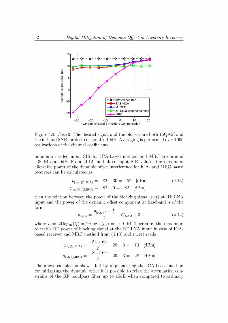
52 Digital Mitigation of Dynamic Offset in Diversity Receivers
−30 −20 −10 0 10 20
−10
−5
0
5
10
15
Average In−Band SIR Before Compensation
Ave
rage
Out
put S
INR
[dB
]
Inteference freeEASI−ICAM−GEFZF Equalization/InversionMRC
Figure 4.3: Case 2: The desired signal and the blocker are both 16QAM andthe in-band SNR for desired signal is 10dB. Averaging is performed over 1000realizations of the channel coefficients.
minimum needed input SIR for ICA-based method and MRC are around−30dB and 0dB. From (4.12) and these input SIR values, the maximumallowable power of the dynamic offset interference for ICA- and MRC-basedreceivers can be calculated as
p|xb(t)|2(ICA) = −82 + 30 = −52 [dBm] (4.13)
p|xb(t)|2(MRC) = −82 + 0 = −82 [dBm]
then the relation between the power of the blocking signal xb(t) at RF LNAinput and the power of the dynamic offset component at baseband is of theform
pxb(t) =p|xb(t)|2 − L
2−GLNA + 3 (4.14)
where L = 20 log10 (lI) = 20 log10 (lQ) = −60 dB. Therefore, the maximumtolerable RF power of blocking signal at the RF LNA input in case of ICA-based receiver and MRC method from (4.13) and (4.14) reads
pxb(t)(ICA) =−52 + 60
2− 20 + 3 = −13 [dBm]
pxb(t)(MRC) =−82 + 60
2− 20 + 3 = −28 [dBm]
The above calculation shows that by implementing the ICA-based methodfor mitigating the dynamic offset it is possible to relax the attenuation con-strains of the RF bandpass filter up to 15dB when compared to ordinary

Spatial Processing Methods 53
MRC processing. In addition, as it is mentioned earlier in this chapter usingthe ICA-based method the overall receiver DSP functionalities are simplifiedcompared to MRC-based receiver in the sense that no channel estimation isneeded in the ICA-based receiver.

54 Digital Mitigation of Dynamic Offset in Diversity Receivers
CHAPTER 5
NONLINEARITY MODELING ANDLINEARIZATION TECHNIQUES IN
RADIO TRANSMITTERS
Communication waveforms with a highly time-variant envelope, like orthog-onal frequency division multiplexing (OFDM) [38], are widely deployed inspectrally efficient digital data transmission links. However, these waveforms,due to their high peak-to-average power ratio (PAPR), impose stringent re-quirements on the linearity of the components in transmitter and receiverchains, most notably on the power amplifier (PA). A nonlinear PA can com-promise the information integrity of the signals with high PAPR and generateexcessive interference in neighboring channels. Thus, to facilitate efficient uti-lization of the available frequency band without interfering with neighboringchannels, a sufficiently linear PA should be deployed in the transmitter. Un-fortunately, the linearity and the power efficiency in PAs are contradictorydesign constrains [18,39,40,69].
One prominent solution to the linearity versus power efficiency dilemmais the utilization of linearizers [69–72], i.e., to implement an efficient nonlin-ear PA in the transmitter but compensate for the nonlinearity effects usingadditional circuitry and/or sophisticated signal processing algorithms. Thischapter includes some essential basics on nonlinear PAs and linearizationtechniques particularly aimed at motivating the reader for the presentationof the main contributions of this manuscript on feedforward linearizationtechnique which is discussed in more detail in Chapters 6 and 7.

56 Nonlinearity Modeling and Linearization Techniques
5.1 Characterizing Input/Output Relation inRF PA
5.1.1 Bussgang Theory
Given a zero-mean Gaussian distributed signal x(t) is the input of an instan-taneous nonlinearity and y(t) is the corresponding output, then according tothe Bussgang theorem [73]
E[y(t)x∗(t)] = αG × E[x(t)x∗(t)] (5.1)
One of the results of this theorem is that the output of an instantaneousnonlinearity with a zero-mean Gaussian distributed input is a scaled versionof the input signal plus an IMD term d(t) that is uncorrelated with the inputsignal i.e.,
y(t) = αGx(t) + d(t) (5.2)
in which E[x(t)d(t−τ)] = 0 ∀τ and the desired signal gain at the nonlinearityoutput is denoted by αG which remains constant for a given variance of thex(t). Although the Bussgang theorem requires Gaussian input signal, it isalso applicable when the distribution of the input signal is close to Gaussian(e.g. OFDM with large number of active subcarriers) [37]. As a result,Bussgang theory is considered a powerful tool in baseband equivalent analysisof communication signals involving nonlinear PA and has been invoked onnumerously in literature [41,46,74,75].
5.1.2 PA Behavioral Modeling
Lets assume signal xRF (t) = A(t) cos(ω0t + ϕ(t)) as the input of an RFPA where A(t) and ϕ(t) are the actual envelope and phase functions of itsequivalent complex baseband signal x(t) = A(t)ejϕ(t). For mathematicaltractability, lets assume a simple third-order polynomial nonlinearity for theRF PA, i.e.
yRF (t) = a1xRF (t) + a2x2RF (t) + a3x
3RF (t)
=a2A
2(t)
2+[a1A(t) +
3a3A3(t)
4
]cos(ω0t+ ϕ(t))
+a2A
2(t)
2cos(2ω0t+ 2ϕ(t)) +
a3A3(t)
4cos(3ω0t+ 3ϕ(t)) (5.3)
where yRF (t) is RF PA output. It is clear from (5.3) that the PA out-
put includes a self-distortion intermodulation term (3a3A3(t)
4) cos(ω0t + ϕ(t))
around input signal center frequency ω0 which interfere with the in-bandsignal. Moreover, with 3 times the bandwidth of the input signal it creates

Characterizing Input/Output Relation in RF PA 57
Figure 5.1: Conceptual demonstration for intermodulation terms generatedas the result of 2nd and third order nonlinearity. The original signal is locatedaround ω0. The fundamental zone and the zonal filter are also depicted inthis figure.
interference close to the original signal center frequency ω0 and on the neigh-boring channels. This phenomenon is referred to in literature as spectralregrowth [18, 40, 60]. The other intermodulation terms in (5.3) are far fromthe original input center frequency as they hit DC, 2ω0, 3ω0, respectively.In modeling RF PAs it is usually assumed that these harmonics of the orig-inal input signal can be safely removed by implementing a linear bandpassfilter [18] also known as zonal filter [76] as the RF frequency is typicallyassumed to be much larger than the largest envelope frequency of the sig-nal. Consequently, the behavioral models, i.e. the models that describe theinput/output relation in the RF PA, are often proposed assuming only theintermodulation terms around and in close vicinity of ω0. This zone in whichthe behavioral models are valid are known in literature as the fundamentalzone (Fig. 5.1.2).Now, considering only the fundamental zone it is clear that the center fre-quency of the RF signal has no influence on the nonlinear behavior of the PAand it is possible to describe the input/output relation of the nonlinearityby the effect of the nonlinearity on the complex envelope of the basebandsignal. The example nonlinearity in (5.3) demonstrates this statement as the
component in the fundamental zone is[a1A(t)+
3a3A3(t)4
]cos(ω0t+ϕ(t)) and
comparing this term to the input RF signal it is possible to describe the non-linearity effect in terms of the complex envelope of the PA input/output. Inthe following we describe such behavioral models which are often used in theliterature. The starting point is the complex baseband equivalent behavioralmodel for a linear PA
y(t) = αLin × x(t) = αLin × A(t)ejϕ(t) (5.4)
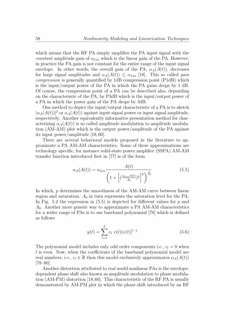
58 Nonlinearity Modeling and Linearization Techniques
which means that the RF PA simply amplifies the PA input signal with theconstant amplitude gain of αLin which is the linear gain of the PA. However,in practice the PA gain is not constant for the entire range of the input signalenvelope. In other words, the overall gain of the PA, αA(A(t)), decreasesfor large signal amplitudes and αA(A(t)) ≤ αLin [18]. This so called gaincompression is generally quantified by 1dB compression point (P1dB) whichis the input/output power of the PA in which the PA gains drops by 1 dB.Of course, the compression point of a PA can be described also, dependingon the characteristic of the PA, by P3dB which is the input/output power ofa PA in which the power gain of the PA drops by 3dB.
One method to depict the input/output characteristic of a PA is to sketch|αA(A(t))|2 or αA(A(t)) against input signal power or input signal amplitude,respectively. Another equivalently informative presentation method for char-acterizing αA(A(t)) is so called amplitude modulation to amplitude modula-tion (AM-AM) plot which is the output power/amplitude of the PA againstits input power/amplitude [18,60].
There are several behavioral models proposed in the literature to ap-proximate a PA AM-AM characteristics. Some of these approximations aretechnology specific, for instance solid-state power amplifier (SSPA) AM-AMtransfer function introduced first in [77] is of the form
αA(A(t)) = αLinA(t)(
1 +[(αLinA(t)
A0)2]p) 1
2p
(5.5)
In which, p determines the smoothness of the AM-AM curve between linearregion and saturation. A0 in turn represents the saturation level for the PA.In Fig. 5.2 the expression in (5.5) is depicted for different values for p andA0. Another more generic way to approximate a PA AM-AM characteristicsfor a wider range of PAs is to use baseband polynomial [78] which is definedas follows
y(t) =L∑l=1
cl x(t)|x(t)|l−1 (5.6)
The polynomial model includes only odd order components i.e., cl = 0 whenl is even. Now, when the coefficients of the baseband polynomial model arereal numbers, i.e., cl ∈ R then this model exclusively approximates αA(A(t))[78–80].
Another distortion attributed to real world nonlinear PAs is the envelope-dependent phase shift also known as amplitude modulation to phase modula-tion (AM-PM) distortion [18,60]. This characteristic of the RF PA is usuallydemonstrated by AM-PM plot in which the phase shift introduced by an RF

Characterizing Input/Output Relation in RF PA 59
PA is sketched against the input signal envelope/power. Considering bothAM-AM and AM-PM distortion, the output of a memoryless nonlinear PAis written as
yRF (t) = αA(A(t)
)cos
(ω0t+ ϕ(t) + ψA(A(t))
)(5.7)
One example from these types of PAs is traveling-wave tube amplifiers (TWTA).A closed-form expression to capture the AM-AM and AM-PM transfer func-tion of TWTA, also known as Saleh model [76, 81], is presented below as
αA(A(t)
)=
χaA(t)
1 + κaA2(t)ψA
(A(t)
)=
χψA2(t)
1 + κψA2(t)(5.8)
in which χa, κa, χψ and κψ are design parameters of Saleh model. ThePAs with AM-AM and AM-PM characteristics can be characterized in moregeneral form using baseband polynomial similar to (5.6) with the differencethat the coefficients cl should be complex numbers [78–80]. Fig.5.3(b), Fig.5.3(a) and Fig. 5.3(c) show the AM-AM, AM-PM and gain vs input signalpower curves for a fifth order approximation of PA characteristic functions.The coefficients of the baseband polynomial are listed below as
c1 = 14.974 + j0.0519
c3 = −27.0954 + j4.9680 (5.9)
c5 = 21.3936 + j0.4305
The underlying assumption for modeling a PA with AM-AM and AM-PMcurve is that the PA AM-AM and AM-PM transfer functions don’t changethroughout the frequency of the operation i.e., αA(A(t)) and ψA(A(t)) areindependent of frequency. Again, in practice and particularly in widebandapplications this assumption is not valid and both gain and phase shift in-troduced by PA are functions of frequency and the input-output relation forthese types of PA is written as
yRF (t) = αA(A(t), ω
)cos
(ω0t+ ϕ(t) + ψA(A(t), ω)
)(5.10)
One example of frequency dependent gain for an actual PA (AG503-86 byWatkins Johnson) is demonstrated in Fig.5.4. The PA output in these typeof PAs doesn’t have instantaneous relation to the PA input and is dependentalso to prior values of the input signal i.e. exhibit memory effect [60, 76].There are numerous attempts to present closed-form expressions for the PAsexhibiting memory effect. One example of these closed-form expressions isthe frequency dependent TWTA model in which all the parameters in (5.8)are assumed to be frequency-dependent and is proposed to model TWTAPAs in wideband applications [81]. Another, rather more general, approach

60 Nonlinearity Modeling and Linearization Techniques
0 1 2 3 4 5 6 7 80
0.5
1
1.5
2
2.5
Input power [dB]
Out
put p
ower
[dB
]
p=1p=2p=3
A0 = 1
A0 = 1.5
Figure 5.2: The AM-AM characteristics of SSPA from (5.5) for differentvalues of p and A0.
to model PAs exhibiting memory effect is to describe their input/outputrelation using Volterra series [76,78].In principle, Volterra series is the most general form of polynomial thatincludes the memory effect. The baseband representation of Volterra seriesconsidering only the fundamental zone of the nonlinearity is as follows [76],
y(t) =
(N+1)/2∑l=1
∫ ∞
−∞
∫ ∞
−∞· · ·
∫ ∞
−∞h2l−1(τ1, τ2, · · · , τ2l−1)dτ1dτ2 · · · dτ2l−1
×l∏
r=1
x(t− τr)2l−1∏p=l+1
x∗(t− τp) (5.11)
in which h2l−1s are low-pass equivalent kernels of the Volterra series, x(t −τr) and x(t − τp) are the delayed version of the input signal and N is thenumber of Volterra kernels which is used in the passband Volterra model. Onemajor issue with modeling nonlinearities in PAs with memory using Volterraseries as such is the large number of coefficients in the model. Therefore, inpractical applications and in particular for modeling nonlinear PAs exhibitingshort-term memory [71, 76] simplified versions of Volterra series are used inwhich some of the Volterra kernels are ignored. Examples of these typesof simplified models are two-box models (e.g., Wiener, Hammerstein) andthree-box models (e.g., Wiener-Hammerstein (WH)). One common aspectof these simplified models is the fact that memory behavior of the nonlineardevice is modeled as linear transfer functions concatenated with a memorylessnonlinearity. For instance, the Wiener model includes a linear filter followed

Characterizing Input/Output Relation in RF PA 61
−12 −10 −8 −6 −4 −2 0−4
−2
0
2
4
6
8
10
P1dB
Input signal power [dB]
Ou
tpu
t si
gn
al p
ow
er
[dB
]
(a) AM-AM characteristics.
−12 −10 −8 −6 −4 −2 0−12
−10
−8
−6
−4
−2
0
2
4
Input signal power [dB]
Ou
tpu
t si
gn
al p
ha
se [
de
g]
(b) AM-PM characteristics.
−14 −12 −10 −8 −6 −4 −2 07.5
8
8.5
9
9.5
10
P1dB
Input signal power [dB]
Am
plif
ier
po
we
r g
ain
[d
B]
(c) Gain vs input signal power.
Figure 5.3: Different characteristic curves for a fifth order approximation ofan actual PA presented in [79]. The P1dB point for this PA is also noted inthis figure.
by a static/memoryless nonlinearity (Fig.5.5(a)) and the baseband equivalentinput/output relation of this model can be described as follows
y(t) = g[h1(t) ∗ x(t)] = g
[ ∫ ∞
−∞h1(τ)x(t− τ)dτ
](5.12)
in which h1(t) is the impulse response of H1, the linear portion of Wienermodel, and g[.] is the static nonlinearity behavioral model. Hammersteinmodel in turn consists of a static nonlinearity followed by a linear filter(Fig.5.5(b)). The input/output relation of Hammerstein model consequentlyreads
y(t) = h2(t) ∗ g[x(t)] =∫ ∞
−∞h1(τ)g[x(t− τ)]dτ (5.13)
in which h2(t) is the impulse response of H2, the linear portion of Hammer-stein model. Finally, Wiener-Hammerstein is the combination of two linear

62 Nonlinearity Modeling and Linearization Techniques
Figure 5.4: Gain dependent behavior of an actual PA (AG503-86) [courtesyof Watkins Johnson].
filters with an static nonlinearity in between, Fig.5.5(c), the input/outputrelation of which reads
y(t) = h2(t) ∗ g[h1(t) ∗ x(t)] =∫ ∞
−∞h2(λ)g
[ ∫ ∞
−∞h1(τ)x(t− λ− τ)dτ
]dλ
(5.14)
Depending on the circuit level information from PA, it is possible to imple-ment one of the specialized models which are already described in this sectione.g., Saleh model as the memoryless nonlinearity g[.]. However, implementingbaseband polynomial (5.6) as the static part provides a more general modelto describe more variety of PAs input/output responses.
5.2 Linearization Techniques
It is already established earlier in this chapter that nonlinear PA in a trans-mitter in general generates self-distorting IMD terms as well as interferenceoutside the transmitting band in the form of spectral regrowth. These in-terfering frequency components are hard to mitigate using linear bandpassfiltering as they are in and close to the desired signal band. On the otherhand, various communication standards restrict the level of distortion thata transmitter inflicts on in-band signal and outside its transmission band.For instance, the maximum level of distortion that a transmitter front-endincluding PA is allowed to create on top of itself is set using error vector
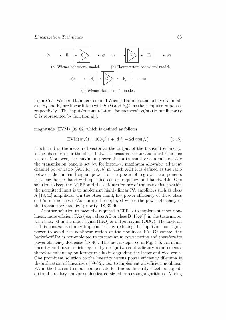
Linearization Techniques 63
(a) Wiener behavioral model. (b) Hammerstein behavioral model.
(c) Wiener-Hammerstein model.
Figure 5.5: Wiener, Hammerstein and Wiener-Hammerstein behavioral mod-els. H1 and H2 are linear filters with h1(t) and h2(t) as their impulse response,respectively. The input/output relation for memoryless/static nonlinearityG is represented by function g[.].
magnitude (EVM) [39,82] which is defined as follows
EVM(in%) = 100√
[1 + |d|2]− 2d cos(ϕe) (5.15)
in which d is the measured vector at the output of the transmitter and ϕeis the phase error or the phase between measured vector and ideal referencevector. Moreover, the maximum power that a transmitter can emit outsidethe transmission band is set by, for instance, maximum allowable adjacentchannel power ratio (ACPR) [39, 76] in which ACPR is defined as the ratiobetween the in band signal power to the power of regrowth componentsin a neighboring band with specified center frequency and bandwidth. Onesolution to keep the ACPR and the self-interference of the transmitter withinthe permitted limit is to implement highly linear PA amplifiers such as classA [18, 40] amplifiers. On the other hand, low power efficiency of these classof PAs means these PAs can not be deployed where the power efficiency ofthe transmitter has high priority [18,39,40].
Another solution to meet the required ACPR is to implement more non-linear, more efficient PAs ( e.g., class AB or class B [18,40]) in the transmitterwith back-off in the input signal (IBO) or output signal (OBO). The back-offin this context is simply implemented by reducing the input/output signalpower to avoid the nonlinear region of the nonlinear PA. Of course, thebacked-off PA is not exploited to its maximum power rating and therefore itspower efficiency decreases [18,40]. This fact is depicted in Fig. 5.6. All in all,linearity and power efficiency are by design two contradictory requirements,therefore enhancing on former results in degrading the latter and vice versa.One prominent solution to the linearity versus power efficiency dilemma isthe utilization of linearizers [69–72], i.e., to implement an efficient nonlinearPA in the transmitter but compensate for the nonlinearity effects using ad-ditional circuitry and/or sophisticated signal processing algorithms. Among
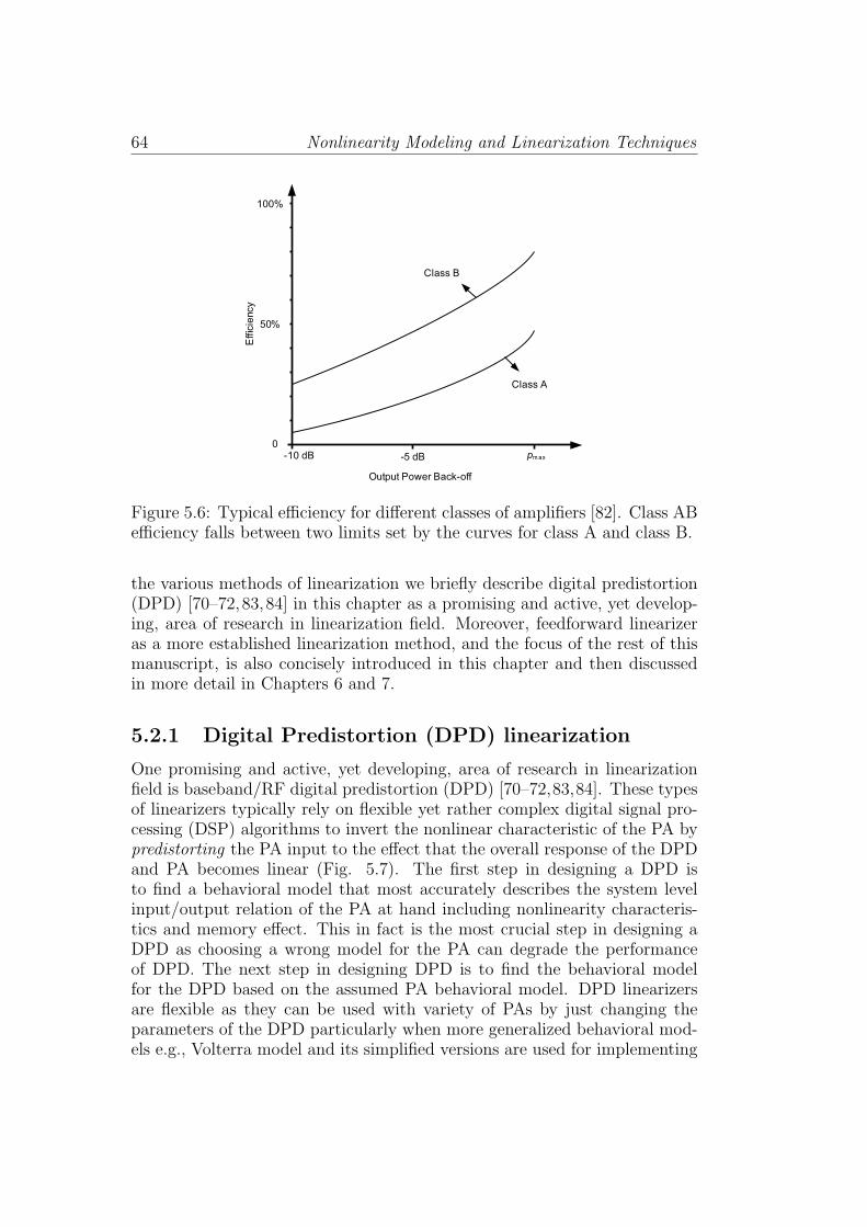
64 Nonlinearity Modeling and Linearization Techniques
Figure 5.6: Typical efficiency for different classes of amplifiers [82]. Class ABefficiency falls between two limits set by the curves for class A and class B.
the various methods of linearization we briefly describe digital predistortion(DPD) [70–72,83,84] in this chapter as a promising and active, yet develop-ing, area of research in linearization field. Moreover, feedforward linearizeras a more established linearization method, and the focus of the rest of thismanuscript, is also concisely introduced in this chapter and then discussedin more detail in Chapters 6 and 7.
5.2.1 Digital Predistortion (DPD) linearization
One promising and active, yet developing, area of research in linearizationfield is baseband/RF digital predistortion (DPD) [70–72,83,84]. These typesof linearizers typically rely on flexible yet rather complex digital signal pro-cessing (DSP) algorithms to invert the nonlinear characteristic of the PA bypredistorting the PA input to the effect that the overall response of the DPDand PA becomes linear (Fig. 5.7). The first step in designing a DPD isto find a behavioral model that most accurately describes the system levelinput/output relation of the PA at hand including nonlinearity characteris-tics and memory effect. This in fact is the most crucial step in designing aDPD as choosing a wrong model for the PA can degrade the performanceof DPD. The next step in designing DPD is to find the behavioral modelfor the DPD based on the assumed PA behavioral model. DPD linearizersare flexible as they can be used with variety of PAs by just changing theparameters of the DPD particularly when more generalized behavioral mod-els e.g., Volterra model and its simplified versions are used for implementing
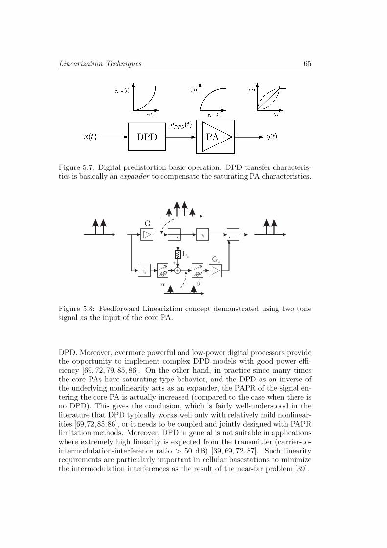
Linearization Techniques 65
Figure 5.7: Digital predistortion basic operation. DPD transfer characteris-tics is basically an expander to compensate the saturating PA characteristics.
G
Ge
Lc
1
2
Figure 5.8: Feedforward Lineariztion concept demonstrated using two tonesignal as the input of the core PA.
DPD. Moreover, evermore powerful and low-power digital processors providethe opportunity to implement complex DPD models with good power effi-ciency [69, 72, 79, 85, 86]. On the other hand, in practice since many timesthe core PAs have saturating type behavior, and the DPD as an inverse ofthe underlying nonlinearity acts as an expander, the PAPR of the signal en-tering the core PA is actually increased (compared to the case when there isno DPD). This gives the conclusion, which is fairly well-understood in theliterature that DPD typically works well only with relatively mild nonlinear-ities [69,72,85,86], or it needs to be coupled and jointly designed with PAPRlimitation methods. Moreover, DPD in general is not suitable in applicationswhere extremely high linearity is expected from the transmitter (carrier-to-intermodulation-interference ratio > 50 dB) [39, 69, 72, 87]. Such linearityrequirements are particularly important in cellular basestations to minimizethe intermodulation interferences as the result of the near-far problem [39].

66 Nonlinearity Modeling and Linearization Techniques
5.2.2 Feedforward Linearizer
The feedforward linearizer is based on the principle of mitigating the in-terfering IMD frequency components by regenerating and subtracting thesecomponents from the PA output at RF. The conceptual diagram of a feed-forward linearizer is depicted in Fig. 5.8. In general, feedforward linearizerPA is unconditionally stable, PA model independent and well suited for mod-ern wideband wireless telecommunication applications [39,41–45]. Moreover,feedforward linearizers can typically handle waveforms with wide bandwidthas well as cases with stringent linearity constraints [39, 69, 85, 87, 88]. Thenext two chapters of this manuscript are devoted to more detailed analysis ofthe feedforward linearizer as well as introducing a novel DSP-oriented feed-forward linearizer concept as a versatile extension of more traditional all-RFlinearizer.
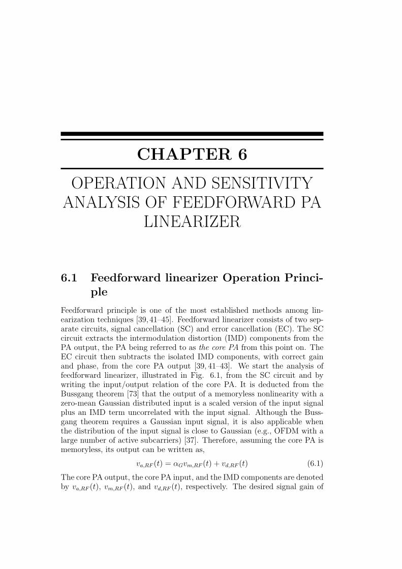
CHAPTER 6
OPERATION AND SENSITIVITYANALYSIS OF FEEDFORWARD PA
LINEARIZER
6.1 Feedforward linearizer Operation Princi-ple
Feedforward principle is one of the most established methods among lin-earization techniques [39, 41–45]. Feedforward linearizer consists of two sep-arate circuits, signal cancellation (SC) and error cancellation (EC). The SCcircuit extracts the intermodulation distortion (IMD) components from thePA output, the PA being referred to as the core PA from this point on. TheEC circuit then subtracts the isolated IMD components, with correct gainand phase, from the core PA output [39, 41–43]. We start the analysis offeedforward linearizer, illustrated in Fig. 6.1, from the SC circuit and bywriting the input/output relation of the core PA. It is deducted from theBussgang theorem [73] that the output of a memoryless nonlinearity with azero-mean Gaussian distributed input is a scaled version of the input signalplus an IMD term uncorrelated with the input signal. Although the Buss-gang theorem requires a Gaussian input signal, it is also applicable whenthe distribution of the input signal is close to Gaussian (e.g., OFDM with alarge number of active subcarriers) [37]. Therefore, assuming the core PA ismemoryless, its output can be written as,
va,RF (t) = αGvm,RF (t) + vd,RF (t) (6.1)
The core PA output, the core PA input, and the IMD components are denotedby va,RF (t), vm,RF (t), and vd,RF (t), respectively. The desired signal gain of

68 Operation and Sensitivity Analysis of Feedforward PA Linearizer
the core PA is αG. Subsequently, the discrete-time baseband equivalent of(6.1) reads
va(n) = αG vm(n) + vd(n) (6.2)
Given perfect delay match between the lower and the upper branches of theSC circuit, the output of the SC circuit yields
ve(n) =√lcva(n)− αvm(n)
=(αG
√lc − α
)vm(n) +
√lcvd(n) (6.3)
The power loss of the attenuator Lc is denoted by lc and the complex valuedcoefficient α represents the gain and the phase rotation provided by thevector modulator in the SC circuit. The SC circuit output is then phase andamplitude corrected using the vector modulator in the EC circuit. Afterwardthe resulting signal is amplified by the error amplifier and finally subtractedfrom the core PA output. Hence, the overall feedforward linearizer outputreads
vo(n) = va(n)− β√geve(n) (6.4)
=(αG
(1− β
√gelc
)+ αβ
√ge
)vm(n) +
(1− β
√gelc
)vd(n)
where the small signal gain of the error amplifier is presented by ge and thecomplex valued coefficient β represents the gain and phase rotation providedby the vector modulator in the EC circuit. Considering the overall outputexpression for the feedforward linearizer in (6.4) the optimum coefficients forthe SC and EC circuits are
αopt = αG√lc
βopt = 1/√gelc (6.5)
These values for α and β maintain the original gain of the core PA and elim-inates the IMD terms at the feedforward linearizer output yielding vo(n) =vo,opt(n) = αGvm(n) [39,41].
6.2 Linearizer Performance Under the SC andEC Coefficient Errors
The optimum coefficients presented in previous section guarantees completemitigation of the IMD terms and preserves the gain of the core PA. However,the optimum values for α and β are functions of the linear gain of the core PA,attenuation of the path in the SC circuit and error amplifier gain, respectively.The nominal values of these circuit parameters are already known, up to the
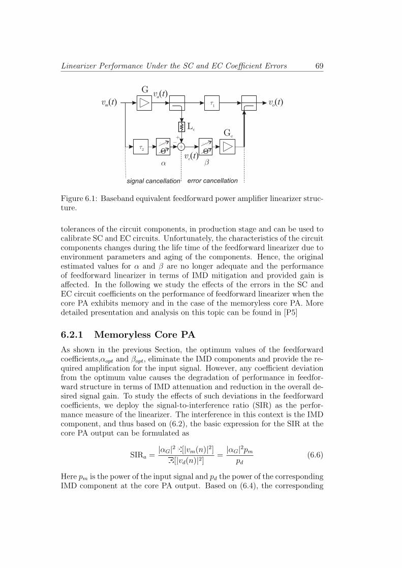
Linearizer Performance Under the SC and EC Coefficient Errors 69
error cancellationsignal cancellation
G
Ge
Lc
vm( )t
va( )t
vo( )t
ve( )t
1
2
Figure 6.1: Baseband equivalent feedforward power amplifier linearizer struc-ture.
tolerances of the circuit components, in production stage and can be used tocalibrate SC and EC circuits. Unfortunately, the characteristics of the circuitcomponents changes during the life time of the feedforward linearizer due toenvironment parameters and aging of the components. Hence, the originalestimated values for α and β are no longer adequate and the performanceof feedforward linearizer in terms of IMD mitigation and provided gain isaffected. In the following we study the effects of the errors in the SC andEC circuit coefficients on the performance of feedforward linearizer when thecore PA exhibits memory and in the case of the memoryless core PA. Moredetailed presentation and analysis on this topic can be found in [P5]
6.2.1 Memoryless Core PA
As shown in the previous Section, the optimum values of the feedforwardcoefficients,αopt and βopt, eliminate the IMD components and provide the re-quired amplification for the input signal. However, any coefficient deviationfrom the optimum value causes the degradation of performance in feedfor-ward structure in terms of IMD attenuation and reduction in the overall de-sired signal gain. To study the effects of such deviations in the feedforwardcoefficients, we deploy the signal-to-interference ratio (SIR) as the perfor-mance measure of the linearizer. The interference in this context is the IMDcomponent, and thus based on (6.2), the basic expression for the SIR at thecore PA output can be formulated as
SIRa =|αG|2E[|vm(n)|2]E[|vd(n)|2]
=|αG|2pmpd
(6.6)
Here pm is the power of the input signal and pd the power of the correspondingIMD component at the core PA output. Based on (6.4), the corresponding

70 Operation and Sensitivity Analysis of Feedforward PA Linearizer
SIR at the overall linearizer output, in turn, is of the form
SIRo =|αG + βα
√ge − βαg
√gelc|2pm
|1− β√gelc|2pd
(6.7)
Clearly, the optimum coefficients αopt and βopt lead to infinite suppression ofIMD, and also any deviation from these optimal values result in imperfectIMD suppression.
Next, in order to explore the relationship between the coefficient deviationand the feedforward linearizer performance, a new measure is introduced.This measure, called relative SIR (r-SIR) in the following, is the ratio betweenSIRo and SIRa and represents the improvement in the signal quality obtainedby employing the linearizer. Now, the expression for this r-SIR can be directlyobtained using (6.6) and (6.7), and reads
r− SIR =SIRo
SIRa
=|αG + βα
√ge − βαG
√gelc|2
|αG|2|1− β√gelc|2
(6.8)
Then, for analysis purposes, we further define the normalized coefficient er-rors of the SC and EC circuits as
ξα =α− αoptαopt
=α
αG√lc− 1
ξβ =β − βoptβopt
= β√lcge − 1 (6.9)
Writing now α and β in terms of the normalized errors ξα and ξβ in (6.8)reads
r− SIR =|1+ξα + ξαξβ|2
|ξβ|2(6.10)
One very interesting conclusion obtained from (6.10) is that the improvementin the SIR, with any reasonable range for ξα and ξβ (i.e. |ξα + ξαξβ| ≪ 1), isdirectly proportional to the reciprocal of |ξβ|2. This, in turn, directly impliesthat the accuracy of the EC circuit coefficient is the critical factor in orderto achieve good linearization performance, while the accuracy requirementfor the SC coefficient is much lower. Moreover, expressing (6.3) in terms ofξα reads
ve(n) = −ξα(αG
√lc
)vm(n) +
√lcvd(n) (6.11)
Therefore, very large errors in ξα causes insufficient attenuation of the mainsignal component in the SC circuit which consequently degrades the efficiencyof the error amplifier and the desired signal gain of the linearizer. It is worthnoting also that in the case where different adaptive or iterative methods

Linearizer Performance Under the SC and EC Coefficient Errors 71
2222
22
2222
2224
24
24
2424
2426
26
26
2626
2628
28
28
2828
2830
30
30
3030
3032
32
32
3232
3234
34
34
3434
34relative amplitude error in β
rela
tive
phas
e er
ror
in β
−0.1 −0.05 0 0.05 0.1
−25
−20
−15
−10
−5
0
5
10
15
20
25
Figure 6.2: Achievable r-SIR levels [in dB] with respect to ξβ. The relativeerror in ξα is 0.2 in amplitude and 10 degree in phase.
are used to obtain the SC and EC loop coefficients simultaneously, errors ordeviations in ξα can also significantly increase the deviations in ξβ [41].
Some example graphical illustrations of the achievable r-SIR levels withexample coefficient deviations of |ξβ| ≤ 0.1, -30 ≤ ∠ξβ ≤ 30 and |ξα|=0.2,∠ξα=10 are presented in Fig. 6.2. Clearly, based on the figure, high r-SIRvalues (and thus high IMD attenuations) are obtainable despite the poor ac-curacy of ξα, as long as the relative errors in β are small (e.g., up to 30 dB forξβ = 5× 10²). This figure also demonstrates that errors in the phase of β donot affect the r-SIR significantly. This is ,of course, clear from (6.10) already.Fig. 6.3, in turn, shows the achievable r-SIR with |ξα| ≤ 0.1, -30 ≤ ∠ξα ≤30 and |ξβ|=0.2, ∠ξβ=10. This clearly verifies and demonstrates theearlier conclusion that the linearizer operation, in terms of IMD reduction(here r-SIR) is fairly robust against inaccuracies in α.
6.2.2 Core PA Exhibiting Memory
In this Section, we extend the analysis of the previous Section to the morepractical case in which the core PA exhibits mild frequency-selectivity in itsresponse, i.e., contains memory. To model such memory in the core PA, thewidely-applied Wiener model, depicted in Figure 6.4, is selected. The Wienermodel is generally a cascade of a linear time-invariant filter (modeling thememory) and a memoryless nonlinearity (modeling the IMD). Now, general-izing the previous derivations, the output of the core PA can first be written

72 Operation and Sensitivity Analysis of Feedforward PA Linearizer
33.233.2
33.2
33.433.4
33.4
33.633.6
33.6
33.8
33.8
33.8
3434
34
34.2
34.234.2
34.4
34.434.4
34.6
34.6
34.6
34.8
relative amplitude error in α
rela
tive
phas
e er
ror
in α
−0.1 −0.05 0 0.05 0.1
−25
−20
−15
−10
−5
0
5
10
15
20
25
Figure 6.3: Achievable r-SIR levels [in dB] with respect to ξα. The relativeerror in ξβ is 0.2 in amplitude and 10 degree in phase.
as
va,RF (t) = αG
∫ +∞
−∞h(τ)vm,RF (t− τ)dτ + vd,RF (t) (6.12)
For analysis purposes, the corresponding causal discrete-time baseband equiv-alent signal is defined as
va(n) = αG
N−1∑k=0
h(k)vm(n− k) + vd(n) (6.13)
For notational convenience in the later analysis, we further assume that thelinear filter h(t) modeling the memory is a normalized minimum phase FIRfilter (i.e., h(0)=1) of length N. This is clearly justified since the frequency-selectivity of practical amplifiers is typically rather mild within any reason-able observation bandwidth. Then, after some fairly straight-forward manip-ulations, the output of the SC circuit can be written as
ve(n) = (α0
√Lc − α)vm(n) +
N−1∑k=1
h(k)vm(n− k) +√Lcvd(n) (6.14)

Linearizer Performance Under the SC and EC Coefficient Errors 73
error cancellationsignal cancellation
G
Ge
Lc
vm( )t
va( )t
vo( )t
ve( )t
H1 1
2
Figure 6.4: Baseband equivalent feedforward power amplifier linearizer struc-ture withe a core PA that exhibits memory. Here the core PA is modeledby concatenation of a finite impulse response (FIR) filter and a memorylessnonlinear function.
Now, substituting (6.13) and (6.14) in (6.4) yields the output of the feedfor-ward structure as
vo(n) = (αG(1− β√gelc) + αβ
√ge)vm(n) (6.15)
+ αG(1− β√gelc)
N−1∑k=1
h(k)vm(n− k) + (1− β√gelc)vd(n)
Here one can notice the interesting fact that setting the feedforward param-eters to the optimum values derived in the case of memoryless PA in Section6.2.1 (i.e. αopt = αG
√lc and βopt = 1/
√gelc), nulls both the IMD as well as
the memory term and also provides the desired amplification for the inputsignal.
Next, in order to define the relationship between the coefficient errors andthe performance of the feedforward linearizer with memory, we determine ther-SIR again in a similar manner as in the memoryless case. First, based on(6.13), the SIR at the output of the core PA reads
SIRa−Wiener =|αG|2pm
|αG|2E[|N−1∑k=1
h(k)vm(n− k)|2]+pd(6.16)
Note that the linear distortion is also treated as interference.The correspond-ing SIR at the feedforward linearizer output is obtained using (6.15) andreads
SIRo−Wiener =1
|1− β√gelc|2
×|αG + βα
√ge − βαG
√gelc|2pm
|αG|2E[|N−1∑k=1
h(k)vm(n− k)|2]+pd(6.17)

74 Operation and Sensitivity Analysis of Feedforward PA Linearizer
Then, the relative SIR (r-SIR) is obtained as the ratio of (6.16) and (6.17),and using also the earlier definitions of ξα and ξβ, is given by
r− SIRWiener=|αG + βα
√ge − βα0
√gelc|2
|αG|2|1− β√gelc|2
=|1+ξα + ξαξβ|2
|ξβ|2(6.18)
which, basically, is the same expression for r− SIR for the memoryless casein 6.10. Note that, in the memory case as opposed to the memoryless case,the interference component is assumed to contain not only the IMD but alsothe memory components (linear distortion). This interpretation of interfer-ence is mainly motivated by the feedforward linearizer concept in which anycomponent at the PA output other than the scaled version of the input signalis considered to be interference and is canceled out at the linearizer output.The expression for r-SIR in (6.8) and (6.18) provides designers with a tool tocalculate the maximum permitted deviation in the adjustment of the SC andEC circuit coefficients depending on the linearization requirement in termsof IMD mitigation. The maximum permitted deviation of the coefficientsin turn have an impact on the choice of estimation algorithm parameters(e.g., step size and number of samples in adaptive algorithms) which is usedin the estimation of these coefficients. One practical application example ofexpressions in (6.8) and (6.18) is presented in [P5].

CHAPTER 7
DSP-ORIENTED FEEDFORWARDAMPLIFIER LINEARIZER
A major obstacle in the way of feedforward linearizer to become the dominantmethod of linearization is the rigid and bulky nature of this structure asit is currently implemented entirely in the RF segment of the transmitterfront-end. This is particularly at odds with recent paradigm-shifting datatransmission system design concepts such as software-defined radio (SDR) [3]and cognitive radio [63].
In the DSP-oriented implementation of feedforward linearizer (DSP-FF)[P2], [P6], on the other hand, the lower branches of EC and SC circuits arecompletely implemented in baseband DSP rather than analog RF. As a result,the IMD components which are needed to linearize the core PA are extractedentirely in the DSP portion of the transmitter. At implementation level,additional demodulator and modulator together with proper data convertersare needed, compared to all-RF feedforward linearizers. It should be noted,however, that also the so-called all-RF linearizers actually utilize similaradditional circuitry and DSP algorithms to calibrate and possibly also trackthe changes of the SC and EC circuit components [41, 43, 46, 89–93]. Thusin this sense, the hardware complexities of the existing linearizers and theproposed one are fairly similar with the difference that here also major partof the core linearization processing is done in DSP.
7.1 DSP-FF Basic Operation Principle
The DSP-FF shown in Fig.7.1 is structurally similar to the all-RF feedforwardlinearizer - it consists of separate SC and EC circuits. However, these circuitsin DSP-FF are implemented partly in DSP regime using I/Q demodulator
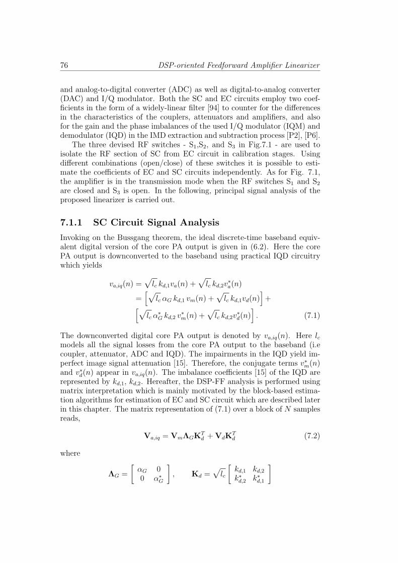
76 DSP-oriented Feedforward Amplifier Linearizer
and analog-to-digital converter (ADC) as well as digital-to-analog converter(DAC) and I/Q modulator. Both the SC and EC circuits employ two coef-ficients in the form of a widely-linear filter [94] to counter for the differencesin the characteristics of the couplers, attenuators and amplifiers, and alsofor the gain and the phase imbalances of the used I/Q modulator (IQM) anddemodulator (IQD) in the IMD extraction and subtraction process [P2], [P6].
The three devised RF switches - S1,S2, and S3 in Fig.7.1 - are used toisolate the RF section of SC from EC circuit in calibration stages. Usingdifferent combinations (open/close) of these switches it is possible to esti-mate the coefficients of EC and SC circuits independently. As for Fig. 7.1,the amplifier is in the transmission mode when the RF switches S1 and S2
are closed and S3 is open. In the following, principal signal analysis of theproposed linearizer is carried out.
7.1.1 SC Circuit Signal Analysis
Invoking on the Bussgang theorem, the ideal discrete-time baseband equiv-alent digital version of the core PA output is given in (6.2). Here the corePA output is downconverted to the baseband using practical IQD circuitrywhich yields
va,iq(n) =√lc kd,1va(n) +
√lc kd,2v
∗a(n)
=[√
lc αG kd,1 vm(n) +√lc kd,1vd(n)
]+[√
lc α∗G kd,2 v
∗m(n) +
√lc kd,2v
∗d(n)
]. (7.1)
The downconverted digital core PA output is denoted by va,iq(n). Here lcmodels all the signal losses from the core PA output to the baseband (i.ecoupler, attenuator, ADC and IQD). The impairments in the IQD yield im-perfect image signal attenuation [15]. Therefore, the conjugate terms v∗m(n)and v∗d(n) appear in va,iq(n). The imbalance coefficients [15] of the IQD arerepresented by kd,1, kd,2. Hereafter, the DSP-FF analysis is performed usingmatrix interpretation which is mainly motivated by the block-based estima-tion algorithms for estimation of EC and SC circuit which are described laterin this chapter. The matrix representation of (7.1) over a block of N samplesreads,
Va,iq = VmΛGKTd +VdK
Td (7.2)
where
ΛG =
[αG 00 α∗
G
], Kd =
√lc
[kd,1 kd,2k∗d,2 k∗d,1
]
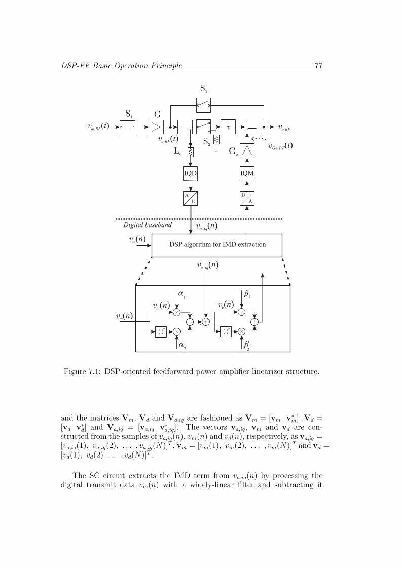
DSP-FF Basic Operation Principle 77
á
S1 G
Ge
Lc
S3
S2
1
2 2
1
vm( )n v
e( )n
ô
â
vm,RF
( )t
va,RF
( )t
vo,RF
DSP algorithm for IMD extraction
IQD IQM
Digital baseband
vm( )n
á â
vm( )n
vGe,RF
( )t
á
va, iq
( )n
va, iq
( )n
Figure 7.1: DSP-oriented feedforward power amplifier linearizer structure.
and the matrices Vm, Vd and Va,iq are fashioned as Vm = [vm v∗m] ,Vd =
[vd v∗d] and Va,iq = [va,iq v∗
a,iq]. The vectors va,iq, vm and vd are con-structed from the samples of va,iq(n), vm(n) and vd(n), respectively, as va,iq =[va,iq(1), va,iq(2), . . . , va,iq(N)]T , vm = [vm(1), vm(2), . . . , vm(N)]T and vd =[vd(1), vd(2) . . . , vd(N)]T .
The SC circuit extracts the IMD term from va,iq(n) by processing thedigital transmit data vm(n) with a widely-linear filter and subtracting it

78 DSP-oriented Feedforward Amplifier Linearizer
from va,iq(n). This is written here as
ve(n) = va,iq(n)− (α1vm(n) + α2v∗m(n))
=[(√
lc αG kd,1 − α1
)vm(n) +
√lc kd,1vd(n)
]+[(√
lc α∗G kd,2 − α2
)v∗m(n) +
√lc kd,2v
∗d(n)
](7.3)
The two coefficients α1 and α2 are implemented in the form of a widely-linearfilter to cancel out the input signal component as well as its conjugate. TheSC circuit output can be written in matrix form following (7.2) and (7.3) as
Ve = Va,iq −VmAT = Vm
(ΛGK
Td −AT
)+VdK
Td (7.4)
where
A =
[α1 α2
α∗2 α∗
1
]The matrix Ve is constructed using the vectors ve and v∗
e as Ve = [ve v∗e ]
in which the vector ve is constructed from the samples of ve(n), i.e., ve =[ve(1), ve(2), . . . , ve(N)]T . The optimum value for the matrix A eliminatesall the input signal components from Va,iq, setting Ve = Ve,opt = VdK
Td or
in signal notations
ve,opt(n) =√lc (kd,1vd(n) + kd,2v
∗d(n)) (7.5)
Therefore, the optimum SC coefficients read from (7.4) as ΛGKTd −AT
opt = Oor
Aopt =
[α1,opt α2,opt
α∗2,opt α∗
1,opt
]= KdΛG (7.6)
Note that ΛG is a diagonal matrix and therefore ΛTG = ΛG. The optimum
values for α1 and α2, from (7.6), are thus
α1,opt =√lcαGkd,1
α2,opt =√lcα
∗Gkd,2 (7.7)
7.1.2 EC Circuit Signal Analysis
The role of EC circuit is to linearly amplify the IMD term which is extractedby SC circuit and to subtract it from the core PA output. A widely-linearfilter with two coefficients, β1 and β2, is utilized also here in EC circuit tocompensate for the finite image attenuation [16] in IQD, from the IMD com-ponent point of view, and in IQM as well as phase/gain imbalance between
DSP-FF Basic Operation Principle 79
Lc and Ge. Therefore, the IMD term at the EC circuit output, or the wholesignal at the EC circuit output when α1 = α1,opt and α2 = α2,opt, reads
vde(n) =√ge
(km,1(β1ve,opt + β2v
∗e,opt) + km,2(β1ve,opt + β2v
∗e,opt)
∗)
= kt,1 vd(n) + kt,2 v∗d(n) (7.8)
The I/Q imbalance coefficients for IQM are represented by km,1 and km,2while the overall I/Q imbalance coefficients of IQD, IQM, and the widely-linear filter in the EC circuit are given by
kt,1 =√lcge
(km,1
(β1kd,1 + β2k
∗d,2
)+ km,2
(β∗1k
∗d,2 + β∗
2kd,1) )
kt,2 =√lcge
(km,1
(β1kd,2 + β2k
∗d,1
)+ km,2
(β∗1k
∗d,1 + β∗
2kd,2) )
(7.9)
Considering blocks of N samples of vde(n) and vd(n), the expression relatingthe IMD term at the PA output and DSP-FF output, presented in (7.8), canbe written in matrix form as
Vde = Vd (KmBKd)T (7.10)
where
B =
[β1 β2β∗2 β∗
1
], Km =
√ge
[km,1 km,2k∗m,2 k∗m,1
]and the matrix Vde = [vde v∗
de] where vde = [vde(1) vde(2) . . . vde(N)]T .The optimum EC circuit coefficients, β1,opt and β2,opt, should cancel out theimbalance effects of IQD and IQM as well as the imbalances between Lc andGe from the IMD components point of view. That means the generated IMDestimate coming from the EC circuit, vde(n), equals the original IMD termvd(n), i.e., vde(n) = vd(n). Thus, based on (7.10), the optimum EC circuitcoefficients fulfill KmBoptKd = I 2×2 meaning
Bopt =
[β1,opt β2,optβ∗2,opt β∗
1,opt
]= K−1
m K−1d (7.11)
The optimum EC coefficients in terms of IQD and IQM imbalance coef-ficients read from (7.11) as
β1,opt =k∗m,1k
∗d,1 + km,2k
∗d,2√
gelc(|km,1|2 − |km,2|2
)(|kd,1|2 − |kd,2|2
)β2,opt = −
k∗m,1kd,2 + km,2kd,1√gelc
(|km,1|2 − |km,2|2
)(|kd,1|2 − |kd,2|2
) (7.12)
80 DSP-oriented Feedforward Amplifier Linearizer
7.2 Least-Squares Methods for SC and ECCoefficient Estimation
In practice, the exact values of lc, αG, and ge as well as the I/Q modu-lator and demodulator imbalance characteristics km,1, km,2, kd,1, and kd,2defining the previously-derived optimum solutions for Aopt and Bopt are allunknown. Thus some practical parameter estimation mechanisms are neededto calibrate the linearizer. Here in this Section, a two-step LS model fittingapproach is proposed. These algorithms are designed to estimate the coeffi-cients of SC and EC circuits independent from each other. As a result, theinaccuracies in the estimation of either coefficients don’t affect the estima-tion of the other set of coefficients. This is an advantage compared to thealgorithms that estimate these coefficients jointly as proposed e.g. in [41],which suffer from this inter-dependance.
One should take note that the estimation methods which are proposed inthe following are, in fact, calibration algorithms and specifically designed forthe initial calibration of the linearizer in production stage. These algorithmscan also be used to track the changes in the circuitry during the normaloperation of the DSP-FF. However, during the estimation period, the datatransmission will be interrupted.
7.2.1 Estimating SC Coefficients α1 and α2
As derived in Section 7.1.1 in (7.6), the optimum SC coefficients α1 andα2 depend on KdΛG. In order to estimate KdΛG using LS model fitting,the principle depicted in Fig. 7.2 is proposed. Here the RF switches S2
and S3 are open while S1 is closed. Note that while open, S2 should beterminated properly to allow the power flow through the preceding couplerwith minimum power reflection (Fig. 7.2). The signal vm,RF (t) is fed tothe core PA. Thereafter the core PA output va,RF (t) is downconverted to thebaseband and digitized. Mα samples of the baseband signals va,iq(n) andvm(n) are stored in two matrices Va,iq and Vm respectively. The relationbetween the two matrices reads from (7.2) and (7.6)
Va,iq = VmATopt +VdK
Td +Vγ (7.13)
The matrix Vγ = [vγ v∗γ] where vγ = [vγ(1), vγ(2), ..., vγ(Mα)]
T and vγ(n)models the baseband digital version of the measurement noise which is as-sumed to be zero-mean, white and Gaussian. Thereafter, the least squares(LS) estimator for Aopt reads
ALS,γ =(V†mVa,iq
)T= Aopt +Kd(V
†mVd)
T + (V†mVγ)
T (7.14)

Least-Squares Methods for SC and EC Coefficient Estimation 81
S2
Lc
S3
S1 G
IQD
v tm,RF
( )
v ta,RF
( )
v nm( ) LS estimation
v na,iq
( )
Figure 7.2: Estimating α1 and α2 in calibration stage.
The behavioral analysis of this estimator in terms of convergence to theoptimum valueAopt in general and for arbitrary values ofMα is not a straightforward task. However, assuming ergodic input signal and measurementnoise, ALS,γ = Aopt when Mα → ∞ [P2]. Rewriting the preceding statementin terms of actual SC circuit coefficients yields,
α∞1,LS = α1,LS
∣∣∣Mα→∞
= α1,opt
α∞2,LS = α2,LS
∣∣∣Mα→∞
= α2,opt (7.15)
7.2.2 Estimating EC Coefficients β1 and β2
Like shown in Subsection 7.1.2 in (7.11) the optimum EC coefficients aredefined by Bopt = K−1
m K−1d . Thus to estimate this product using again LS
model fitting, the setup depicted in Fig.7.3 is proposed here. In this setup, S3 is closed while S1 and S2 are open. A test signal, vin(n), is injectedinto the modulator branch of EC circuit. The signal which is used for thetransmission can be equally well used as the test signal here. The test signalis then downconverted to the baseband and is digitized using IQD and ADC,respectively. The relation between the input and output test signals is then

82 DSP-oriented Feedforward Amplifier Linearizer
LSestimation
S2
ô
GS1
Ge
Lc
vin( )nv
out( )n
Digital baseband
S3
Figure 7.3: Estimating β1 and β2 in calibration stage.
given by
vout(n) =√gelc
((kd,1km,1 + kd,2k
∗m,2)vin(n) + (kd,1km,2 + kd,2k
∗m,1)v
∗in(n)
)(7.16)
Thereafter, Mβ samples of the input and the output test signals are stored invin = [vin(1), vin(2), ..., vin(Mβ)]
T and vout = [vout(1), vout(2), ..., vout(Mβ)]T ,
respectively. Finally, the matrices Vin = [vin v∗in] and Vout = [vout v
∗out] are
formed. Including the measurement noise term Vγ, the matrix Vout can nowbe written in terms of Vin as
Vout = Vin(KdKm)T +Vγ (7.17)
and the estimator for EC coefficients yields then
BLS,γ = (V†outVin)
T =
((Vin (KdKm)
T +Vγ
)†Vin
)T
(7.18)
The detailed analysis in [P2] reveals that this estimator doesn’t convergeto the desired value even when Mβ → ∞. The underlying cause of thisperformance degradation is that the measurement noise in this estimatorcreates error in Vout as this matrix is formed from the samples of vout(n).Therefore, the problem at hand is different from typical LS where the errors
DSP-FF Linearization Performance Analysis 83
are considered only in the observed vector or in our case Vin. These typesof LS problems, known as errors-in-variables or Data Least-Squares (DLS),have been addressed widely in the literature in other applications [95, 96].Here, the induced large sample coefficient estimation errors are defined as
ϵ∞β,1 = β1,LS
∣∣∣Mβ→∞
− β1,opt
ϵ∞β,2 = β2,LS
∣∣∣Mβ→∞
− β2,opt (7.19)
These errors are direct functions of the optimum EC coefficients, IQD andIQM I/Q imbalance coefficients as well as the signal-to-measurement-noiseratio. Closed form expressions for ϵ∞β,1 and ϵ
∞β,2 are presented in the following
[P2].
Σ∞B =
det((KdKm)
∗(KdKm)T)
det((KdKm)∗(KdKm)T +Υ−1
SNR,in
) − 1
Bopt
+(KdKm)
HΥ−1SNR,in
det((KdKm)∗(KdKm)T +Υ−1
SNR,in
) (7.20)
where
Σ∞B =
[ϵ∞β,1 ϵ∞β,2
(ϵ∞β,2)∗ (ϵ∞β,1)
∗
], ΥSNR,in =
[ pinpγ
0
0 pinpγ
]Here, pin and pγ are the powers of the input test signal and measurementnoise,respectively.
7.3 DSP-FF Linearization Performance Anal-ysis
The main function of DSP-FF is to mitigate the IMD components generatedby the core PA. Hence, the ratio between the power of IMD distortion com-ponent at the core PA output and DSP-FF output is a natural measure forthe performance of DSP-FF. We refer to this measure as intermodulationattenuation ratio (IMDAr). The detail analysis in [P2] shows that undercircularity assumption on the IMD term, i.e. E[v2d(n)] = 0, and for Mβ → ∞the IMDAr reads
IMDAr
∣∣Mβ→∞ = IMDA∞
r =pdpd,o
=1/gelc∣∣km,1kd,1ϵ∞β,1 + km,1kd,2(ϵ∞β,2)
∗∣∣2 + ∣∣k∗m,2kd,1ϵ∞β,2 + k∗m,2kd,2(ϵ
∞β,1)
∗∣∣2 (7.21)

84 DSP-oriented Feedforward Amplifier Linearizer
where pd and pd,o are the IMD distortion powers at the core PA and DSP-FFoutput respectively. It is interesting to note here that IMDA∞
r is independentof the error in the SC coefficients. Moreover, as it is already mentioned in7.2.2, closed form expression for ϵ∞β,1 and ϵ
∞β,2 and their conjugate are available
in (7.20). Therefore, for given DSP-FF circuit parameters - ge, lc,kd,1,kd,2,km,1and km,2 - and signal-to-measurement noise ratio, the IMDA∞
r is analyticallypredictable using (7.21).
Although IMDAr is representative for the main function of DSP-FF,i.e.IMD distortion mitigation, it can not alone paint a complete picture foroverall performance of this linearizer. Nevertheless, a large IMDAr alwaysindicates that the IMD distortion components at the DSP-FF output is prop-erly mitigated. However, large IMDAr may also be achieved by merelyimplementing input/output power back-off which defeats the very idea ofimplementing the DSP-FF and results in poor overall power efficiency [40].Therefore, a measure representing the relation between the input and outputpower of the DSP-FF, hand in hand with IMDAr, provides complete insightinto DSP-FF performance. Such a measure is defined here as the gain of theDSP-FF for the desired signal. Ideally, the DSP-FF gain should be equal tothe desired signal gain provided by the core PA. However, any error in the es-timation of DSP-FF circuit coefficients, especially the SC circuit coefficients,degrade the desired signal gain. Fortunately, as the large sample analysis ofthe SC circuit estimator shows in (7.15), α∞
1,LS = α1,opt and α∞2,LS = α2,opt.
Therefore, for sufficiently large number of samples used in the estimationof SC circuit coefficients the DSP-FF and the core PA desired signal gainsare equal. For more detailed analysis of the effects of SC and EC coefficienterrors on the DSP-FF gain please refer to [P2].
7.3.1 Operation and Performance Under Core PA withMemory
The above analysis on the operation of DSP-FF and the performance of theEC and SC coefficients estimators can be extended to the case where the corePA exhibits memory. The detailed treatments of these topics are providedin [P2]. Here, we provide only the essential conclusions and outcomes of theanalysis in [P2]. Firstly it is shown in [P2] that the memory characteristics ofthe core doesn’t have any effect on the optimum coefficients of the EC circuitand the EC optimum coefficients in case of the core PA with memory areidentical to the memoryless case. Moreover, the analysis presented in [P2]shows the errors in estimation of the EC coefficients are independent of thecore PA memory and in both memory and memoryless case can be expressedwith (7.20).
The IMDA∞r for DSP-FF with the core PA which is modeled by WH

DSP-FF Linearization Performance Analysis 85
behavioral model (Fig. 5.5(c)) reads [P2]
IMDAwh,∞r =
pwhdpwh,∞d,o
(7.22)
The superscript wh denotes the signal values and variables in DSP-FF anal-ysis for the case of the PA with Wiener-Hammerstein behavioral model. Thepower of the IMD terms at the WH PA and DSP-FF output are denotedhere by pwhd and pwh,∞d,o , respectively. All in all, with a circularity assump-tion for the IMD term, i.e. E[vd (n) vd (n+ l)] = 0 ∀ l, and some straightforward math it is possible to show that IMDAwh,∞
r = IMDA∞r [P2]. Here,
one should pay especial attention to the fact that IMDAwh,∞r represents the
amount of reduction in the power of the IMD component and its delayed(filtered) versions.
The SC circuit analysis in the case of the core with memory, where thebehavioral model of the PA is again assumed to be WH, shows that theoptimum values for SC circuit coefficients are in the following form [P2]
Awhopt = KdΛGHd
T (7.23)
where HdT is defined as
HdT =
[hT (d) 00 h∗T (d)
]Here, hT (n) = h1(n) ∗ h2(n) where h1(n) and h2(n) are the finite impulseresponse (FIR) pre- and post-filter impulse responses of the WH model, re-spectively, d is the delay of the overall WH structure in samples and ∗ is theconvolution operator. The same setup as the memoryless case can be usedto estimate the optimum SC coefficients. In particular case of WH core PAthe LS estimator for SC coefficients reads [P2]
AwhLS =
(V†m,LT−d Va,iq
)T(7.24)
where Vm,LT−d = [vm,LT−dv∗m,LT−d] where the vector vm,LT−d = [vm(LT −
d + 1), . . . , vm(LT +Mα − d)]T and LT is the number of taps in hT (n). Itis demonstrated through analysis in [P2] that SC coefficients estimator Awh
LS
approaches to its optimum values as the number of samples which is used inthe estimation grows sufficiently large, i.e. Awh,∞
LS = Awhopt, even in presence
of measurement noise. As the result, similar to the memoryless case, theoverall gain of the WH PA is preserved by DSP-FF linearizer [P2].
86 DSP-oriented Feedforward Amplifier Linearizer
7.4 Simulation and Numerical Examples
The first set of experiments is performed to verify and demonstrate the an-alytical results on the errors in the estimation of β1 and β2 in the presenceof measurement noise which is stated in Subsection 7.2.2. It follows then byanother experiment verifying the analytical expression for IMDA∞
r in (7.21).The second batch of experiments verifies the analytical results on the SCcircuit coefficients estimation error and their effect on the DSP-FF desiredsignal gain which was presented in Section 7.3. The signals which are usedthrough out these experiments are OFDM signals with 1024 subcarriers ofwhich 300 are active around the center-frequency except for the DC bin.The memoryless core PA which is used in the simulations is modeled by abaseband polynomial [79] of the form
y(n) =L∑l=1
cl x(n)|x(n)|l−1 (7.25)
The polynomial model includes only odd order components i.e. cl = 0 whenl is even. The coefficients values are taken from a class AB power amplifiermodel [79]
c1 = 14.974 + j0.0519
c3 = −27.0954 + j4.9680 (7.26)
c5 = 21.3936 + j0.4305
A WH is used in the simulations involving a core PA with memory. Thestatic part of the WH model in this simulations is a SSPA model [77] withp = 2 and the clipping level of A0 = 1. The pre- and post-filter in thisWH model are complex-valued infinite impulse response (IIR) filters of thefollowing form
H1(z) =(1 + 0.2j) + (0.3 + 0.1j)z−1
(1 + 0.1j) + (−0.2 + 0.05j)z−1
H2(z) =(1 + 0.2j) + (0.3 + 0.1j)z−2
(1 + 0.1j) + (0.2 + 0.05j)z−2(7.27)
Finally, the imbalance values for IQD and IQM are 5%, 6, 6% and 7,respectively, which represent a realistic example scenario.
7.4.1 EC Circuit Coefficients Error and IMDAr: Mem-oryless Core PA
The curves in Fig. 7.4 represent the errors in the estimation of EC circuitcoefficients. The simulated curves are obtained for different sample numbers
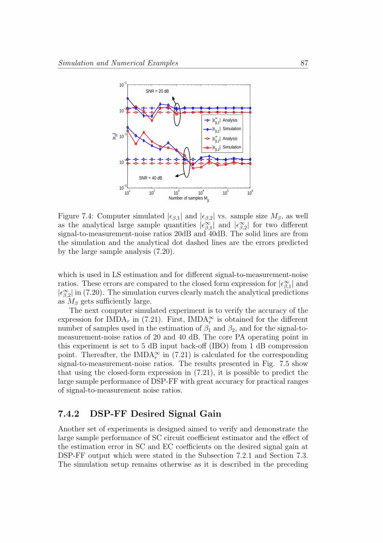
Simulation and Numerical Examples 87
101
102
103
104
105
106
10−5
10−4
10−3
10−2
10−1
Number of samples Mβ
|εβ|
|ε∞β,1
| Analysis
|εβ,1| Simulation
|ε∞β,2
| Analysis
|εβ,2| Simulation
SNR = 40 dB
SNR = 20 dB
Figure 7.4: Computer simulated |ϵβ,1| and |ϵβ,2| vs. sample size Mβ, as wellas the analytical large sample quantities |ϵ∞β,1| and |ϵ∞β,2| for two differentsignal-to-measurement-noise ratios 20dB and 40dB. The solid lines are fromthe simulation and the analytical dot dashed lines are the errors predictedby the large sample analysis (7.20).
which is used in LS estimation and for different signal-to-measurement-noiseratios. These errors are compared to the closed form expression for |ϵ∞β,1| and|ϵ∞β,2| in (7.20). The simulation curves clearly match the analytical predictionsas Mβ gets sufficiently large.
The next computer simulated experiment is to verify the accuracy of theexpression for IMDAr in (7.21). First, IMDA∞
r is obtained for the differentnumber of samples used in the estimation of β1 and β2, and for the signal-to-measurement-noise ratios of 20 and 40 dB. The core PA operating point inthis experiment is set to 5 dB input back-off (IBO) from 1 dB compressionpoint. Thereafter, the IMDA∞
r in (7.21) is calculated for the correspondingsignal-to-measurement-noise ratios. The results presented in Fig. 7.5 showthat using the closed-form expression in (7.21), it is possible to predict thelarge sample performance of DSP-FF with great accuracy for practical rangesof signal-to-measurement noise ratios.
7.4.2 DSP-FF Desired Signal Gain
Another set of experiments is designed aimed to verify and demonstrate thelarge sample performance of SC circuit coefficient estimator and the effect ofthe estimation error in SC and EC coefficients on the desired signal gain atDSP-FF output which were stated in the Subsection 7.2.1 and Section 7.3.The simulation setup remains otherwise as it is described in the preceding

88 DSP-oriented Feedforward Amplifier Linearizer
101
102
103
104
105
106
20
30
40
50
60
70
80
Number of samples Mβ
IMD
Ar [d
B]
SNR = 40 dB (Simulation)
SNR = 40 dB (Analytical)
SNR = 20 dB (Simulation)
SNR = 20 dB (Analytical)
Figure 7.5: IMDAr vs. number of samples Mβ used in the LS estimatorfor β1 and β2. The experiment is performed for 20dB and 40dB signal-to-measurement-noise ratios. The operation point of the core PA is 5dB IBOfrom 1dB compression point. The solid lines are the results of computersimulations and the dashed lines are analytical results obtained from (7.21).
subsection. In the first experiment, the estimation of SC circuit coefficientsis performed as described in Subsection 7.2.1. The estimation of α1 and α2 isperformed under two different signal-to-measurement noise ratios, 20 dB and40 dB. The core PA is operated at 5 dB IBO from its 1 dB compression point.The number of samples which are used to estimate SC coefficients is variedfrom 10 to 106. The results of this experiment in Fig. 7.6 show that theerrors in α1,LS and α2,LS are significantly reduced as the number of samplesreaches 103 and practically vanishes when the number of samples approaches106. This experiment also demonstrates that the measurement noise doesnot affect the performance of the estimator. This result is again clearly inline with the large sample analysis of the EC circuit estimator presented inSubsection 7.2.1. In the second experiment, the desired signal gain of theDSP-FF is simulated. The core PA is operated at 5, 8 and 10 dB IBO from1 dB compression point. The number of samples used in the estimation ofthe SC coefficients is varied from 10 to 106. The estimation of α1 and α2 isperformed for two different values of signal-to-measurement-noise ratios, 20dB and 40 dB. The results of this experiments presented in Fig. 7.7 depictthe desired signal gain of the DSP-FF and the core PA against each other. Itis observed from this figure that the DSP-FF gain for desired signal matchesthe core PA desired signal gain when Mα is sufficiently large, independent

Simulation and Numerical Examples 89
102
103
104
105
106
3
4
5
|α1|
|α1,LS
| 40 dB SNR
|α1,LS
| 20 dB SNR
|α1,opt
|
102
103
104
105
106
0
0.2
0.4
0.6
0.8
Number of samples Mα
|α2|
|α2,LS
| 40 dB SNR
|α2,LS
| 20 dB SNR
|α2,opt
|
Figure 7.6: Computer simulated |α1,LS| and |α2,LS| against |α1,opt| and |α2,opt|for different number of samplesMα used in the SC circuit LS estimator. Thesignal-to-measurement-noise ratios are 20dB and 40dB and the operationpoint of the core PA is 5dB IBO from 1dB compression point.
of measurement noise level. This is again in line with the earlier analyticalresults. One should also note that according to these results, the effect oferrors in the estimation of β1,LS and β2,LS is insignificant as the number ofsamples to estimate EC circuit coefficients is here only 100 and the signal-to-measurement-noise ratio is set to 20 dB which yields high estimation errorsin the order of 10−2 in the EC circuit coefficients (Fig.7.4).
7.4.3 IMDAr and DSP-FF Overall Gain: WH PA
This set of simulated experiments is designed to demonstrates IMDAr andoverall gain performance of the DSP-FF when the core PA exhibits memoryeffect. The setup for the experiment is identical to the previously describedsimulations with a difference that the core PA is the WH model which isdescribed at the beginning of this section. The input signal power is setin such a way that the SSPA model is driven at 3 dB compression pointto ensure extreme nonlinear behavior. The outcomes of the experimentspresented in Fig. 7.8 and Fig. 7.9 verify that the closed-from expressionsof (7.20) and (7.21) are equally valid for a core PA with memory. This iswell in line with the results already stated in Subsection 7.3.1. The powerspectrum of the PA output and the corresponding DSP-FF output for onerealization of the above described experiment is depicted in Fig. 7.10 forillustration purposes. The LS coefficients are estimated under 40dB signal-to-measurement-noise ratio. The number of samples used in LS estimations

90 DSP-oriented Feedforward Amplifier Linearizer
102
103
104
105
106
9
10
11
12
13
14
15
Number of samples Mα
|Gai
n| [l
inea
r sc
ale]
Desired signal gain (PA)Desired signal gain (DSP−FF) 40 dB SNRDesired signal gain (DSP−FF) 20 dB SNR
IBO = 5 dB
IBO = 8 dB
IBO = 10 dB
Figure 7.7: Desired signal gain of the core PA and the overall DSP-FF struc-ture vs. number of samples Mα used in the SC circuit LS estimator. Theresults are depicted for 5dB, 8dB and 10dB IBOs from 1dB compressionpoint of the core PA. The signal-to-measurement-noise ratios in estimationof α1 and α2 are 20dB (star) and 40dB (diamond). The estimation of β1 andβ2 is always performed under signal-to-noise ratio of 20dB with Mβ = 100samples.
are 105 and 100 for EC and SC circuits, respectively. The comparison of thecore PA output power spectrum and the linearized one shows that the DSP-FF in use effectively mitigates the IMD components. One should also notethat due to EC circuit coefficients estimation inaccuracies, stemming frommeasurement noise, the IMD components are not entirely eliminated. Thus,since the core PA exhibits memory, also the remaining IMD componentscontain memory, which in turn manifest itself as the residual memory effectsvisible in Fig. 7.10. As predicted with analysis, Fig. 7.11 confirms that thelarge sample estimation of SC circuit coefficients indeed converge to theiroptimum values in case of a core PA with memory. The preservation of thecore PA desired signal gain for a memory PA, which is again predicted withanalysis, is also depicted in Fig. 7.12.
7.4.4 Laboratory Measurement Experiment
A measurement setup is also devised to demonstrate the performance ofthe DSP-FF with real-world electronics. A PA is driven, first, close to itsmaximum output power rating which creates high levels of spectral regrowthat the core PA output. Thereafter, using DSP-FF, the attenuation of thespectral regrowth is demonstrated.
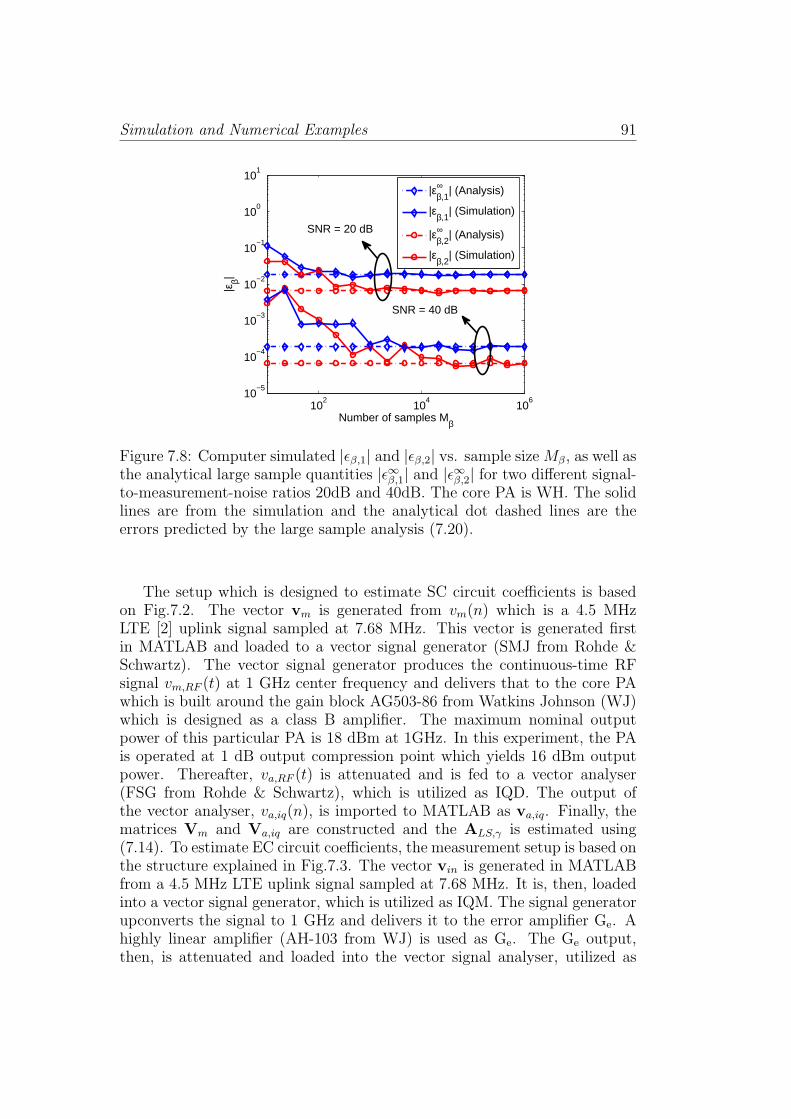
Simulation and Numerical Examples 91
102
104
106
10−5
10−4
10−3
10−2
10−1
100
101
Number of samples Mβ
|εβ|
|ε∞β,1
| (Analysis)
|εβ,1| (Simulation)
|ε∞β,2
| (Analysis)
|εβ,2| (Simulation)
SNR = 40 dB
SNR = 20 dB
Figure 7.8: Computer simulated |ϵβ,1| and |ϵβ,2| vs. sample sizeMβ, as well asthe analytical large sample quantities |ϵ∞β,1| and |ϵ∞β,2| for two different signal-to-measurement-noise ratios 20dB and 40dB. The core PA is WH. The solidlines are from the simulation and the analytical dot dashed lines are theerrors predicted by the large sample analysis (7.20).
The setup which is designed to estimate SC circuit coefficients is basedon Fig.7.2. The vector vm is generated from vm(n) which is a 4.5 MHzLTE [2] uplink signal sampled at 7.68 MHz. This vector is generated firstin MATLAB and loaded to a vector signal generator (SMJ from Rohde &Schwartz). The vector signal generator produces the continuous-time RFsignal vm,RF (t) at 1 GHz center frequency and delivers that to the core PAwhich is built around the gain block AG503-86 from Watkins Johnson (WJ)which is designed as a class B amplifier. The maximum nominal outputpower of this particular PA is 18 dBm at 1GHz. In this experiment, the PAis operated at 1 dB output compression point which yields 16 dBm outputpower. Thereafter, va,RF (t) is attenuated and is fed to a vector analyser(FSG from Rohde & Schwartz), which is utilized as IQD. The output ofthe vector analyser, va,iq(n), is imported to MATLAB as va,iq. Finally, thematrices Vm and Va,iq are constructed and the ALS,γ is estimated using(7.14). To estimate EC circuit coefficients, the measurement setup is based onthe structure explained in Fig.7.3. The vector vin is generated in MATLABfrom a 4.5 MHz LTE uplink signal sampled at 7.68 MHz. It is, then, loadedinto a vector signal generator, which is utilized as IQM. The signal generatorupconverts the signal to 1 GHz and delivers it to the error amplifier Ge. Ahighly linear amplifier (AH-103 from WJ) is used as Ge. The Ge output,then, is attenuated and loaded into the vector signal analyser, utilized as

92 DSP-oriented Feedforward Amplifier Linearizer
102
104
106
20
30
40
50
60
70
80
Number of samples Mβ
IMD
Ar [d
B]
SNR = 40 (Simulation)SNR = 40 (Analysis)SNR = 20 (Simulation)SNR = 20 (Analysis)
Figure 7.9: IMDAr vs. number of samples Mβ used in the LS estimatorfor β1 and β2 for WH core PA. The experiment is performed for 20dB and40dB signal-to-measurement-noise ratios. The solid lines are the results ofcomputer simulations and the dashed lines are analytical results obtainedfrom (7.21).
IQD. The vector vout is configured in MATLAB using the samples of vout(n),which is the vector analyser output. Next, the matrices Vin and Vout areconstructed from the vectors vin and vout, respectively. Finally, BLS,γ isestimated using (7.18).
The final step of the experiment consists of two stages: first generatingthe baseband error signal and second subtracting the generated error signalfrom the core PA output.
For the first stage, another realization of the vector vm is generated inMATLAB and loaded into the vector signal generator. The vector signalgenerator upconverts the signal to 1 GHz, then the upconverted signal is fedto the core PA. Thereafter the core PA output is attenuated, downconvertedand loaded to MATLAB. Now, the baseband error vector, ve, is estimatedfrom (7.4). The error vector is processed in Matlab by the estimated ECcircuit coefficients and is then upconverted to 1 GHz using the vector signalgenerator. The upconverted error signal is amplified by Ge and finally sub-tracted from the core PA output. The resulting signal is DSP-FF output,vo,RF (t). A variable RF delay is utilized after the core PA to ensure that thesubtraction at the core PA output is performed with acceptable delay match.The core PA input, the core PA output and the resulting DSP-FF outputare presented in Fig. 7.13. In this case, the number of samples which is usedfor the estimation of SC and EC circuit coefficients is 104. The DSP-FF in
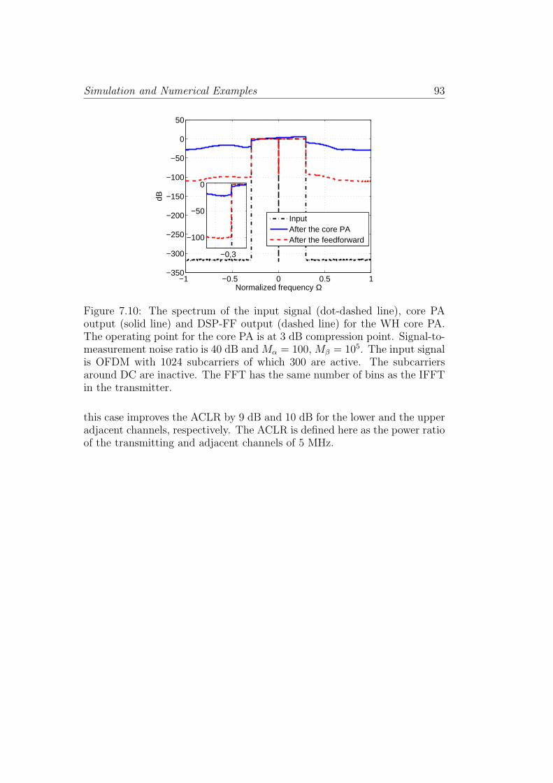
Simulation and Numerical Examples 93
−1 −0.5 0 0.5 1−350
−300
−250
−200
−150
−100
−50
0
50
Normalized frequency Ω
dB
−0,3
−100
−50
0
InputAfter the core PAAfter the feedforward
Figure 7.10: The spectrum of the input signal (dot-dashed line), core PAoutput (solid line) and DSP-FF output (dashed line) for the WH core PA.The operating point for the core PA is at 3 dB compression point. Signal-to-measurement noise ratio is 40 dB andMα = 100,Mβ = 105. The input signalis OFDM with 1024 subcarriers of which 300 are active. The subcarriersaround DC are inactive. The FFT has the same number of bins as the IFFTin the transmitter.
this case improves the ACLR by 9 dB and 10 dB for the lower and the upperadjacent channels, respectively. The ACLR is defined here as the power ratioof the transmitting and adjacent channels of 5 MHz.

94 DSP-oriented Feedforward Amplifier Linearizer
102
104
106
0
5
10
Number of samples Mα
|α2|
|αwh2,LS
| 40 dB SNR
|αwh2,LS
| 20 dB SNR
|αwh2,opt
|
102
104
106
10
15
20
25
30
35
|α1|
|αwh1,LS
| 40 dB SNR
|αwh1,LS
| 20 dB SNR
|αwh1,opt
|
Figure 7.11: Computer simulated |αwh1,LS| and |αwh2,LS| against |αwh1,opt| and
|αwh2,opt| for different number of samples Mα used in the SC circuit LS es-timator for WH core PA. The signal-to-measurement-noise ratios are 20dBand 40dB and the operating point of the core PA is 0dB IBO from 3dBcompression point.
102
104
106
40
50
60
70
80
90
100
|Gai
n| [l
inea
r sc
ale]
Number of samples Mα
Desired signal gain (PA)Desired signal gain (DSP−FF) 40 dB SNRDesired signal gain (DSP−FF) 20 dB SNR
IBO = 0 dB
IBO = 3 dB
Figure 7.12: Desired signal gain of the core PA and the overall DSP-FFstructure vs. number of samples Mα used in the SC circuit LS estimator andfor WH core PA. The results are depicted for 0dB and 3 dB IBOs from 3dBcompression points of the core PA. The signal-to-measurement-noise ratios inestimation of α1 and α2 are 20dB (star) and 40dB (diamond). The estimationof β1 and β2 is always performed under signal-to-noise ratio of 20dB withMβ
= 100 samples.

Simulation and Numerical Examples 95
−10 −8 −6 −4 −2 0 2 4 6 8 10−50
−45
−40
−35
−30
−25
−20
−15
−10
−5
0
5
Frequency [MHz]
dB
The core PA outputDSP−FF outputThe core PA input
Figure 7.13: Measured normalized power spectrum of the core PA input, thecore PA output and DSP-FF output. An LTE uplink signal with 4.5 MHzbandwidth is used in this laboratory measurement. The solid line representsthe power spectrum of the linearized signal. The dotted line presents thecore PA output and the dashed line is the core PA input. The number ofsamples which is used to estimate SC and EC circuit coefficients is 104. Thex-axis represents the frequencies around 1 GHz center frequency.

96 DSP-oriented Feedforward Amplifier Linearizer

CHAPTER 8
CONCLUSIONS
Dirty-RF concept, i.e., mixed signal processing/DSP algorithms to compen-sate for the front-end non-ideality effects, plays a crucial role in shapingthe future of radio transceiver design. Deploying dirty-RF-based algorithmsenables transceiver designers to design power efficient, wideband, portableand yet affordable radio devices through the use of less-than-perfect front-end components. Naturally, designing algorithms based on dirty-RF conceptrequires familiarity with the design strategies and algorithms which are gen-erally used on either side of the ADC. In addition, proper understanding ofcertain non-ideality effects is an essential requirement for devising an effec-tive strategy to mitigate those effects. That was the main ideology shapingup the structure of this manuscript, i.e. first to understand the effects ofnonlinearity in radio transceivers, as the non-ideality which was the focus ofthis thesis, and then to propose proper dirty-RF-inspired DSP solutions tomitigate the nonlinearity effects in radio transceivers.
In the early parts of this manuscript the effects of nonlinearity in thecontext of DCR was studied. In particular the effects of nonlinear LNA andnonlinearity in I/Q path of the DCR was analyzed. As the result the profileof spurious frequency components for both types of nonlinearity was derived.As one of the contributions of this manuscript, it was shown that the nonlin-earity in the I/Q branches of the DCR downconversion path generate ratherdifferent spurious frequency profile compared to LNA. This was presentedin general through formal analysis of real passband nonlinearity (for LNA)and I/Q passband nonlinearity (for the I/Q paths of DCR). Based on thederived interference profile a DSP-based adaptive interference cancellation(IC) method was proposed to mitigate the interfering components stemmingfrom the combined effects of nonlinear LNA and nonlinear elements in I/Qbranches. Laboratory measurement experiments using real world telecom-munications signals and actual receiver front-end showed that the proposed
98 Conclusions
IC method significantly mitigates these interfering terms.
The dynamic DC-offset problem in multiple-front-end DCR was treatednext in this manuscript. The dynamic DC-offset components, resulting fromRF signal self-mixing hit the desired signal band and are particularly dam-aging when they are created from self-mixing of strong blockers. Here, thesignal model for the dynamic DC-offset for multiple-front-end receiver wasderived. Furthermore, DSP algorithm based on ICA was proposed to miti-gate the effects of dynamic DC-offset interference in the multiple front-endDCR. Deploying this DSP method relaxes the requirement on the isolationlevels between the mixing core ports and therefore less expensive mixers canbe deployed in DCR. Simulation results comparing the proposed algorithmagainst a number of bench mark diversity algorithms showed the superiorinterference mitigation of this method in a wide range of SNR.
The combined nonlinearity analysis of all the nonlinear elements in DCRand possible compensation method for transmitter nonlinearity implementedin the receiver side and detailed analysis of the proposed algorithm in combi-nation to other non-idealities in the receiver are among future topics. More-over, analysis of the effects of non-idealities in general and nonlinearity inparticular on the sensing algorithms and actual CR receivers are among thepromising and exciting topics.
On the transmitter side the nonlinearity study was focused mostly on themajor source of nonlinearity in the radio transmitters, i.e., the RF poweramplifier (PA). The system-level modeling of PA, i.e., behavioral modeling,was explained. Thereafter, the linearity vs. power efficiency dilemma in thePA design was presented to motivate the linearization topic, and in particularfeedforward linearizer, as a solution which strikes a balance between linearityand power efficiency in PA. The effects of the errors in the adjustments offeedforward linearizer coefficients on the performance of this linearizer wereanalyzed. A closed-form expression relating these errors and linearizationperformance of feedforward linearizer with memoryless core PA in terms ofr-SIR, i.e., the improvement in the signal-to-interference ratio as the resultof deploying a feedforward linearizer, was derived.
To improve the flexibility of the feedforward linearizer, a DSP-orientedimplementation of feedforward linearizer was proposed in this thesis. Inthis implementation of the feedforward linearizer major parts of its principalfunctionality, i.e., generation of the error signal, is transferred to the DSPregime. In addition, block-based algorithms to estimate the EC and SC coef-ficients were proposed. These algorithms have the benefits of estimating ECand SC coefficients independently, i.e., the error in the estimation of one ofthe coefficients doesn’t propagate to the other coefficient. The large sampleanalysis of the EC circuit coefficients estimator revealed that the presenceof measurement noise limits the accuracy of the EC circuit coefficient esti-mator. A closed-form expression predicting the large-sample EC coefficient
99
estimation error was derived analytically. The error in the estimation of ECcoefficients in turn affects the linearization performance of DSP-FF in termsof the attenuation of intermodulation distortion. This performance measurewas described as IMDAr, or the ratio between the IMD term power at thePA output and DSP-FF output. In addition, a closed-form expression de-scribing IMDAr in terms of DSP-FF parameters was derived analytically.The above analyses were also extended for the DSP-FF with a core PA ex-hibiting memory. Extensive computer simulation results were reported toverify and demonstrate the analytical results for both cases where the corePA exhibits memory and the memoryless case. Finally, a proof-of-conceptmeasurement setup demonstrated the achieved spectral regrowth suppressionby this structure.
Among the future directions on the feedforward linearizer studies, aredesigning an adaptive algorithm to track the changes in the SC and ECcircuit parameters and implementing more advanced algorithms at the base-band process of DSP-FF to improve its performance and power efficiency.Moreover, it is possible to show that in case IQM and IQD exhibit frequencydependent I/Q imbalances, those effects can be also compensated using simi-lar approach as presented in this manuscript. The only required modificationis to replace the coefficients in EC and SC circuits widely-linear filters withmultitap filters. The in-depth analysis of such structure as well as introduc-ing proper method to estimate these filters are considered in future studies.In the greater scheme of nonlinearity studies in transmitters, studies on im-proving the performance of digital predistorters, as a promising linearizerstructure, as well as analyzing and compensating the combined effect of allthe non-idealities in the transmitter chain will have great academic and socialimpact in future.

100 Conclusions

CHAPTER 9
SUMMARY OF PUBLICATIONSAND AUTHOR’S CONTRIBUTIONS
In this chapter we briefly describe the contents of the original publications[P1]-[P6]. The contributions of the thesis author to each individual publica-tion contents are also discussed.
9.1 Summary of Publications
In [P1] and [P4], the contributions of nonlinear analog front-end in generatinginter/cross-modulations interference on top of the desired signal in the pres-ence of multiple strong signals are analyzed. In this analysis nonlinearities inLNA as well as nonlinear elements in the I/Q branches of a DCR receiver areconsidered, presenting the input/output relation of these elements using a ba-sic polynomial model. The result of the derivations shows a distinct featurefor the interference profile generated by nonlinear LNA and I/Q nonlinearelements. Based on the derived interference profile a DSP-based adaptiveinterference cancellation method is proposed to mitigate the interfering com-ponents stemming from the combined effect of nonlinear LNA and nonlinearelements in I/Q branches. Laboratory measurement experiments using realworld telecommunications signals and actual receiver front-end show that theproposed IC method significantly mitigates these interfering terms.
The issue of DCR with dynamic DC-offset in multiple-front-end receiverscontext is studied in [P3]. Dynamic DC-offset components are generated asthe result of RF signal self-mixing from insufficient isolation between the RFand LO port of the mixing core. Furthermore, DSP algorithm based on ICAis proposed in [P3] to mitigate the effects of dynamic DC-offset componentinterference in multiple front-end DCR. Simulation results comparing the

102 Summary of Publications and Author’s Contributions
proposed algorithm against a number of bench mark diversity algorithmssuch as zero-forcing ZF and MRC shows the superior interference mitigationcapability of this method in a wide range of SNR.
The effects of the errors in the adjustments of feedforward linearizer coef-ficients on the linearization performance are analyzed in [P5]. A closed-formexpression relating these errors and linearization performance of feedforwardlinearizer with memoryless core PA in terms of r-SIR, i.e., the improvementin the signal-to-interference ratio as the result of deploying feedforward lin-earizer, is derived. It is shown analytically that the same expression for r-SIRcan be equally used for the case where the core PA in feedforward linearizerexhibits memory effects.
One major drawback of the feedforward linearizer is that it is typicallyimplemented entirely in the RF regime using bulky and rigid components.Therefore to improve upon this aspect of feedforward a DSP-oriented imple-mentation of feedforward linearizer (DSP-FF) is initially proposed in [P6].Least-square-based estimation algorithms for calibrating SC and EC circuitsare also proposed in [P6]. These algorithms have the benefits of estimat-ing EC and SC coefficients independently, i.e., the error in the estimationof one of the coefficients doesn’t propagate to the other coefficient. Thor-ough performance analysis of DSP-FF as well as implementation aspects ofDSP-FF are presented in [P2]. Modified and improved estimation methodsfor SC and EC circuits, in comparinson with [P6] are introduced in [P2].The large sample performance of SC and EC coefficients estimators in thecase of a memoryless core PA under and in the presence of measurementnoise are analyzed. As a result a closed-form expression predicting the ECcoefficient estimation floor performance is derived analytically. Moreover, aperformance measure for DSP-FF, i.e., IMDAr or the ratio between the IMDterm power at the PA output and DSP-FF output is introduced in [P2]. Aclosed-form expression describing IMDAr in terms of DSP-FF componentsparameters is presented in [P2]. The above analyses are also extended for theDSP-FF with a core PA with memory. Extensive computer simulation re-sults are reported to verify the analytical results for both cases where the corePA exhibits memory and the memoryless case. Finally, a proof-of-conceptmeasurement setup demonstrates the achieved interference mitigation by thisstructure.
9.2 Author’s Contributions to the Publica-tions
The entire research work reported in publications [P1]-[P6] was carried outin the Department of Communications Engineering (DCE), Tampere Uni-versity of Technology (TUT), Finland, Tampere. The idea for the adaptive

Author’s Contributions to the Publications 103
interference cancellation method resulting in publications [P1] and [P4] wasinitially proposed by the supervisor, Prof. Mikko Valkama, and Prof. MarkkuRenfors. In [P4], the author performed the analysis leading to the new un-derstanding of the interference profile of the I/Q bandpass nonlinearity. Thesimulation and measurement experiments as well as the preparation of themanuscript were performed by the author. The supervisor guided the authorthrough all the mentioned tasks and also contributed significantly to the fi-nal appearance of the manuscript. In [P1], the author performed the bulk ofthe analytical derivations, simulation experiments and laboratory measure-ment. Incorporating memory effect in the interference cancellation structurewas proposed and implemented by the author. The final manuscript wasprepared in collaboration with the supervisor, the author of the thesis con-tributed in writing of analytical and results sections. The application of ICAin mitigating dynamic DC-offset reported in [P3], was proposed by the au-thor. The signal modeling, design of the simulation experiments and writingthe manuscript was solely performed by the author. The sensitivity anal-ysis of feedforward linearizer leading to the publication [P5] was proposedby the author. The author was the main contributor to this publication.The DSP-oriented implementation of feedforward linearizer was the result ofcollaboration between DCE and Institute of Communications and Informa-tion Engineering, University of Linz, Austria and Danube Integrated CircuitsEngineering (DICE). The final structure for DSP-FF was the result of closecollaborations between the author of the thesis and M.Sc. Sascha Burglech-ner from University of Linz. In [P6] the signal modeling, estimation algorithmdesign and simulation experiments are designed by the author. The authoralso contributed to the writing of the final manuscript particularly bulk of thetheoretical section. In publication [P2] the author was the main contributor.In all the analytical results, simulation experiments and in preparation ofthe manuscript the author of this thesis was the main contributor. However,the measurement experiment was performed in collaboration with the secondauthor. All in all, prof. Mikko Valkama made essential contributions in allthe publications through insightful comments and useful suggestions.
9.2.1 Other Publications by The Author
In addition to the publications which are included in this manuscript theauthor contributed to a number of other articles closely related to the topicof the thesis. These articles are not included in the manuscript, however theyare cited in the reference section as [33,34,47,97,98].

104 Summary of Publications and Author’s Contributions
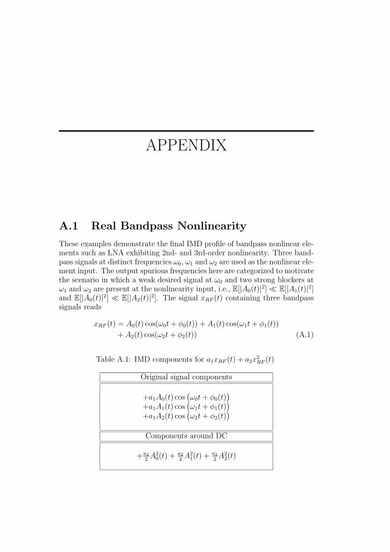
APPENDIX
A.1 Real Bandpass Nonlinearity
These examples demonstrate the final IMD profile of bandpass nonlinear ele-ments such as LNA exhibiting 2nd- and 3rd-order nonlinearity. Three band-pass signals at distinct frequencies ω0, ω1 and ω2 are used as the nonlinear ele-ment input. The output spurious frequencies here are categorized to motivatethe scenario in which a weak desired signal at ω0 and two strong blockers atω1 and ω2 are present at the nonlinearity input, i.e., E[|A0(t)|2] ≪ E[|A1(t)|2]and E[|A0(t)|2] ≪ E[|A2(t)|2]. The signal xRF (t) containing three bandpasssignals reads
xRF (t) = A0(t) cos(ω0t+ ϕ0(t)) + A1(t) cos(ω1t+ ϕ1(t))
+ A2(t) cos(ω2t+ ϕ2(t)) (A.1)
Table A.1: IMD components for a1xRF (t) + a2x2RF (t)
Original signal components
+a1A0(t) cos(ω0t+ ϕ0(t)
)+a1A1(t) cos
(ω1t+ ϕ1(t)
)+a1A2(t) cos
(ω2t+ ϕ2(t)
)Components around DC
+a22A2
0(t) +a22A2
1(t) +a22A2
2(t)
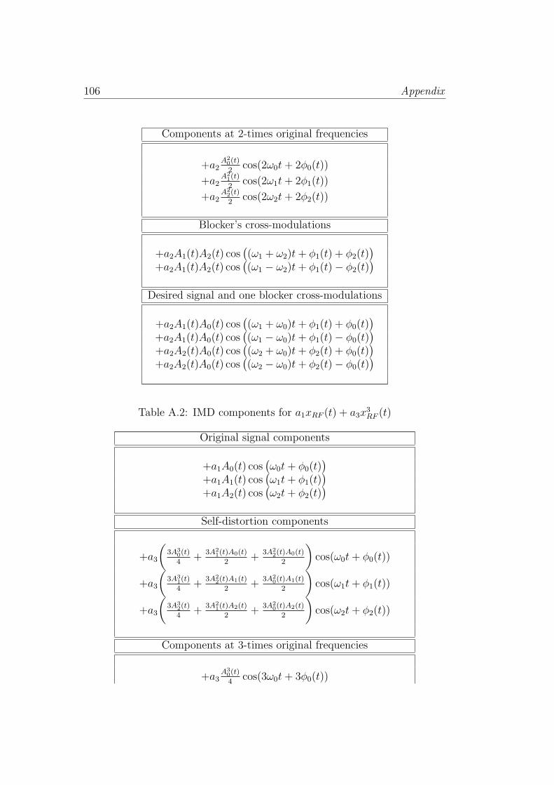
106 Appendix
Components at 2-times original frequencies
+a2A2
0(t)
2cos(2ω0t+ 2ϕ0(t))
+a2A2
1(t)
2cos(2ω1t+ 2ϕ1(t))
+a2A2
2(t)
2cos(2ω2t+ 2ϕ2(t))
Blocker’s cross-modulations
+a2A1(t)A2(t) cos((ω1 + ω2)t+ ϕ1(t) + ϕ2(t)
)+a2A1(t)A2(t) cos
((ω1 − ω2)t+ ϕ1(t)− ϕ2(t)
)Desired signal and one blocker cross-modulations
+a2A1(t)A0(t) cos((ω1 + ω0)t+ ϕ1(t) + ϕ0(t)
)+a2A1(t)A0(t) cos
((ω1 − ω0)t+ ϕ1(t)− ϕ0(t)
)+a2A2(t)A0(t) cos
((ω2 + ω0)t+ ϕ2(t) + ϕ0(t)
)+a2A2(t)A0(t) cos
((ω2 − ω0)t+ ϕ2(t)− ϕ0(t)
)
Table A.2: IMD components for a1xRF (t) + a3x3RF (t)
Original signal components
+a1A0(t) cos(ω0t+ ϕ0(t)
)+a1A1(t) cos
(ω1t+ ϕ1(t)
)+a1A2(t) cos
(ω2t+ ϕ2(t)
)Self-distortion components
+a3
(3A3
0(t)
4+
3A21(t)A0(t)
2+
3A22(t)A0(t)
2
)cos(ω0t+ ϕ0(t))
+a3
(3A3
1(t)
4+
3A22(t)A1(t)
2+
3A20(t)A1(t)
2
)cos(ω1t+ ϕ1(t))
+a3
(3A3
2(t)
4+
3A21(t)A2(t)
2+
3A20(t)A2(t)
2
)cos(ω2t+ ϕ2(t))
Components at 3-times original frequencies
+a3A3
0(t)
4cos(3ω0t+ 3ϕ0(t))

I/Q Bandpass Nonlinearity 107
+a3A3
1(t)
4cos(3ω1t+ 3ϕ1(t))
+a3A3
2(t)
4cos(3ω2t+ 3ϕ2(t))
Blocker’s cross-modulations
+a33A2
1(t)A2(t)
4cos((2ω1 + ω2)t+ 2ϕ1(t) + ϕ2(t))
+a33A2
1(t)A2(t)
4cos((2ω1 − ω2)t+ 2ϕ1(t)− ϕ2(t))
+a33A2
2(t)A1(t)
4cos((2ω2 + ω1)t+ 2ϕ2(t) + ϕ1(t))
+a33A2
2(t)A1(t)
4cos((2ω2 − ω1)t+ 2ϕ2(t)− ϕ1(t))
Desired signal and one blocker cross-modulations
+a33A2
1(t)A0(t)
4cos((2ω1 + ω0)t+ 2ϕ1(t) + ϕ0(t))
+a33A2
1(t)A0(t)
4cos((2ω1 − ω0)t+ 2ϕ1(t)− ϕ0(t))
+a33A2
0(t)A1(t)
4cos((2ω0 + ω1)t+ 2ϕ0(t) + ϕ1(t))
+a33A2
0(t)A1(t)
4cos((2ω0 − ω1)t+ 2ϕ0(t)− ϕ1(t))
+a33A2
2(t)A0(t)
4cos((2ω2 + ω0)t+ 2ϕ2(t) + ϕ0(t))
+a33A2
2(t)A0(t)
4cos((2ω2 − ω0)t+ 2ϕ2(t)− ϕ0(t))
+a33A2
0(t)A2(t)
4cos((2ω0 + ω2)t+ 2ϕ0(t) + ϕ2(t))
+a33A2
0(t)A2(t)
4cos((2ω0 − ω2)t+ 2ϕ0(t)− ϕ2(t))
Desired signal and both blockers cross-modulations
+a36A0(t)A1(t)A2(t)
4cos((ω1 − ω2 − ω0)t+ ϕ1(t)− ϕ2(t)− ϕ0(t))
+a36A0(t)A1(t)A2(t)
4cos((ω1 − ω2 + ω0)t+ ϕ1(t)− ϕ2(t) + ϕ0(t))
+a36A0(t)A1(t)A2(t)
4cos((ω1 + ω2 − ω0)t+ ϕ1(t) + ϕ2(t)− ϕ0(t))
+a36A0(t)A1(t)A2(t)
4cos((ω1 + ω2 + ω0)t+ ϕ1(t) + ϕ2(t) + ϕ0(t))
A.2 I/Q Bandpass Nonlinearity
These examples demonstrate the final complex IMD profile of nonlinearitiesin I and Q branches of a radio receiver based on I/Q downconverion principleexhibiting 2nd- and 3rd-order nonlinearity. Three complex signals at distinctfrequencies ω0, ω1 and ω2 are used as the nonlinearity input. Moreover, topresent a realistic and more general scenario the nonlinearities in I and Qbranches exhibit different characteristics. The output spurious frequencieshere are categorized to motivate the scenario in which a weak desired signal at

108 Appendix
ω0 and two strong blockers at ω1 and ω2 are present at the nonlinearity inputi.e. E[|A0(t)|2] ≪ E[|A1(t)|2] and E[|A0(t)|2] ≪ E[|A2(t)|2]. The signal modelfor I and Q elements of downconverted signal x(t) which contain three signalswith distinct frequencies passing through nonlinear elements are presentedin the following tables.
x(t) = A0(t)ej(ω0t+ϕ0(t)) + A1(t)e
j(ω1t+ϕ1(t)) + A2(t)ej(ω2t+ϕ2(t)) (A.2)
Table A.3: IMD components for b1xI(t) + b2x2I(t) +
j[g1b1xQ(t) + g2b2x2Q(t)]
Original signal components
+b11+g12A0(t)e
j(ω0t+ϕ0(t))
+b11−g12A0(t)e
−j(ω0t+ϕ0(t))
+b11+g12A1(t)e
j(ω1t+ϕ1(t))
+b11−g12A1(t)e
−j(ω1t+ϕ1(t))
+b11+g12A2(t)e
j(ω2t+ϕ2(t))
+b11−g12A2(t)e
−j(ω2t+ϕ2(t))
Components around DC
+b2(1 + jg2)[A2
0(t)
2+
A21(t)
2+
A22(t)
2]
Components at ±2-times original frequencies
+b21−jg2
4
A20(t)
2ej(2ω0t+2ϕ0(t))
+b21−jg2
4
A20(t)
2e−j(2ω0t+2ϕ0(t))
+b21−jg2
4
A21(t)
2ej(2ω1t+2ϕ1(t))
+b21−jg2
4
A21(t)
2e−j(2ω1t+2ϕ1(t))
+b21−jg2
4
A22(t)
2ej(2ω2t+2ϕ2(t))
+b21−jg2
4
A22(t)
2e−j(2ω2t+2ϕ2(t))
Blocker’s cross-modulations
+b21−jg2
2A1(t)A2(t)e
j((ω1+ω2)t+ϕ1(t)+ϕ2(t))
+b21−jg2
2A1(t)A2(t)e
−j((ω1+ω2)t+ϕ1(t)+ϕ2(t))
+b21+jg2
2A1(t)A2(t)e
j((ω1−ω2)t+ϕ1(t)−ϕ2(t))
+b21+jg2
2A1(t)A2(t)e
−j((ω1−ω2)t+ϕ1(t)−ϕ2(t))

I/Q Bandpass Nonlinearity 109
Desired signal and one blocker cross-modulations
+b21−jg2
2A1(t)A0(t)e
j((ω1+ω0)t+ϕ1(t)+ϕ0(t))
+b21−jg2
2A1(t)A0(t)e
−j((ω1+ω0)t+ϕ1(t)+ϕ0(t))
+b21+jg2
2A1(t)A0(t)e
j(ω1−ω0)t+ϕ1(t)−ϕ0(t)
+b21+jg2
2A1(t)A0(t)e
−j(ω1−ω0)t+ϕ1(t)−ϕ0(t)
+b21−jg2
2A2(t)A0(t)e
j(ω2+ω0)t+ϕ2(t)+ϕ0(t)
+b21−jg2
2A2(t)A0(t)e
−j(ω2+ω0)t+ϕ2(t)+ϕ0(t)
+b21+jg2
2A2(t)A0(t)e
j(ω2−ω0)t+ϕ2(t)−ϕ0(t)
+b21+jg2
2A2(t)A0(t)e
−j(ω2−ω0)t+ϕ2(t)−ϕ0(t)
Table A.4: IMD components for b1xI(t) + b3x3I(t) +
j[g1b1xQ(t) + g3b3x
3Q(t)
]Original signal components
+b11+g12A0(t)e
j(ω0t+ϕ0(t))
+b11−g12A0(t)e
−j(ω0t+ϕ0(t))
+b11+g12A1(t)e
j(ω1t+ϕ1(t))
+b11−g12A1(t)e
−j(ω1t+ϕ1(t))
+b11+g12A2(t)e
j(ω2t+ϕ2(t))
+b11−g12A2(t)e
−j(ω2t+ϕ2(t))
Self-distortion components
+ b3(1+g3)2
(3A3
0(t)
4+
3A21(t)A0(t)
2+
3A22(t)A0(t)
2
)ej(ω0t+ϕ0(t))
+ b3(1+g3)2
(3A3
1(t)
4+
3A22(t)A1(t)
2+
3A20(t)A1(t)
2
)ej(ω1t+ϕ1(t))
+ b3(1+g3)2
(3A3
2(t)
4+
3A21(t)A2(t)
2+
3A20(t)A2(t)
2
)ej(ω2t+ϕ2(t))
IMD Components at original signals mirror frequency
+ b3(1−g3)2
(3A3
0(t)
4+
3A21(t)A0(t)
2+
3A22(t)A0(t)
2
)e−j(ω0t+ϕ0(t))
+ b3(1−g3)2
(3A3
1(t)
4+
3A22(t)A1(t)
2+
3A20(t)A1(t)
2
)e−j(ω1t+ϕ1(t))

110 Appendix
+ b3(1−g3)2
(3A3
2(t)
4+
3A21(t)A2(t)
2+
3A20(t)A2(t)
2
)e−j(ω2t+ϕ2(t))
Components at ±3-times original frequencies
+ b3(1−g3)2
A30(t)
4ej(3ω0t+3ϕ0(t))
+ b3(1+g3)2
A30(t)
4e−j(3ω0t+3ϕ0(t))
+ b3(1−g3)2
A31(t)
4ej(3ω1t+3ϕ1(t))
+ b3(1+g3)2
A31(t)
4e−j(3ω1t+3ϕ1(t))
+ b3(1−g3)2
A32(t)
4ej(3ω2t+3ϕ2(t))
+ b3(1+g3)2
A32(t)
4e−j(3ω2t+3ϕ2(t))
Blocker’s cross-modulations
+ b3(1−g3)2
3A21(t)A2(t)
4ej((2ω1+ω2)t+2ϕ1(t)+ϕ2(t))
+ b3(1+g3)2
3A21(t)A2(t)
4e−j((2ω1+ω2)t+2ϕ1(t)+ϕ2(t))
+ b3(1+g3)2
3A21(t)A2(t)
4ej((2ω1−ω2)t+2ϕ1(t)−ϕ2(t))
+ b3(1−g3)2
3A21(t)A2(t)
4e−j((2ω1−ω2)t+2ϕ1(t)−ϕ2(t))
+ b3(1−g3)2
3A22(t)A1(t)
4ej((2ω2+ω1)t+2ϕ2(t)+ϕ1(t))
+ b3(1+g3)2
3A22(t)A1(t)
4e−j((2ω2+ω1)t+2ϕ2(t)+ϕ1(t))
+ b3(1+g3)2
3A22(t)A1(t)
4ej((2ω2−ω1)t+2ϕ2(t)−ϕ1(t))
+ b3(1−g3)2
3A22(t)A1(t)
4e−j((2ω2−ω1)t+2ϕ2(t)+ϕ1(t))
Desired signal and one blocker cross-modulations
+ b3(1−jg3)2
3A21(t)A0(t)
4ej((2ω1+ω0)t+2ϕ1(t)+ϕ0(t))
+ b3(1+jg3)2
3A22(t)A1(t)
4e−j((2ω1+ω0)t+2ϕ2(t)+ϕ1(t))
+ b3(1+jg3)2
3A21(t)A0(t)
4ej((2ω1−ω0)t+2ϕ1(t)−ϕ0(t))
+ b3(1−jg3)2
3A22(t)A1(t)
4e−j((2ω1−ω0)t+2ϕ2(t)+ϕ1(t))
+ b3(1−jg3)2
3A20(t)A1(t)
4ej((2ω0+ω1)t+2ϕ0(t)+ϕ1(t))
+ b3(1+jg3)2
3A22(t)A1(t)
4e−j((2ω0+ω1)t+2ϕ2(t)+ϕ1(t))
+ b3(1+jg3)2
3A20(t)A1(t)
4ej((2ω0−ω1)t+2ϕ0(t)−ϕ1(t))
+ b3(1−jg3)2
3A22(t)A1(t)
4e−j((2ω0−ω1)t+2ϕ2(t)+ϕ1(t))
+ b3(1−jg3)2
3A22(t)A0(t)
4ej((2ω2+ω0)t+2ϕ2(t)+ϕ0(t))
+ b3(1+jg3)2
3A22(t)A1(t)
4e−j((2ω2+ω0)t+2ϕ2(t)+ϕ1(t))
+ b3(1+jg3)2
3A22(t)A0(t)
4ej((2ω2−ω0)t+2ϕ2(t)−ϕ0(t))

I/Q Bandpass Nonlinearity 111
+ b3(1−jg3)2
3A22(t)A1(t)
4e−j((2ω2−ω0)t+2ϕ2(t)+ϕ1(t))
+ b3(1−jg3)2
3A20(t)A2(t)
4ej((2ω0+ω2)t+2ϕ0(t)+ϕ2(t))
+ b3(1+jg3)2
3A22(t)A1(t)
4e−j((2ω0+ω2)t+2ϕ2(t)+ϕ1(t))
+ b3(1+jg3)2
3A20(t)A2(t)
4ej((2ω0−ω2)t+2ϕ0(t)−ϕ2(t))
+ b3(1−jg3)2
3A22(t)A1(t)
4e−j((2ω0−ω2)t+2ϕ2(t)+ϕ1(t))
Desired signal and both blockers cross-modulations
+ b3(1−jg3)2
6A0(t)A1(t)A2(t)4
ej((ω1−ω2−ω0)t+ϕ1(t)−ϕ2(t)−ϕ0(t))
+ b3(1+jg3)2
6A0(t)A1(t)A2(t)4
e−j((ω1−ω2−ω0)t+ϕ1(t)−ϕ2(t)−ϕ0(t))
+ b3(1+jg3)2
6A0(t)A1(t)A2(t)4
ej((ω1−ω2+ω0)t+ϕ1(t)−ϕ2(t)+ϕ0(t))
+ b3(1−jg3)2
6A0(t)A1(t)A2(t)4
e−j((ω1−ω2+ω0)t+ϕ1(t)−ϕ2(t)+ϕ0(t))
+ b3(1+jg3)2
6A0(t)A1(t)A2(t)4
ej((ω1+ω2−ω0)t+ϕ1(t)+ϕ2(t)−ϕ0(t))
+ b3(1−jg3)2
6A0(t)A1(t)A2(t)4
e−j((ω1+ω2−ω0)t+ϕ1(t)+ϕ2(t)−ϕ0(t))
+ b3(1−jg3)2
6A0(t)A1(t)A2(t)4
ej((ω1+ω2+ω0)t+ϕ1(t)+ϕ2(t)+ϕ0(t))
+ b3(1+jg3)2
6A0(t)A1(t)A2(t)4
e−j((ω1+ω2+ω0)t+ϕ1(t)+ϕ2(t)+ϕ0(t))

112 Appendix

BIBLIOGRAPHY
[1] Near Field Communication Interface and Protocol, ECMA-340; seconded., 2004.
[2] Evolved Universal Terrestrial Radio Access (E-UTRA) ; Physical Chan-nels and Modulation, 3GPP TS 36.211 V9.1.0, 2010.
[3] J. Mitola, “The software radio architecture,” IEEE Commun. Magazine,vol. 33, no. 5, pp. 26–38, May 1995.
[4] S. Haykin, “Cognitive radio: brain-empowered wireless communica-tions,” IEEE J. Selected Areas in Comm., vol. 23, no. 2, pp. 201 –220, feb 2005.
[5] D. Cabric and R. W. Brodersen, “Physical layer design issues unique tocognitive radio systems,” in Proc. IEEE Int. Symp. on Personal, Indoorand Mob. Radio Comm. (PIMRC), vol. 2, 2005, pp. 759–763.
[6] B. Razavi, “Cognitive radio design challenges and techniques,” IEEE J.Solid-State Circuits, vol. 45, no. 8, pp. 1542–1553, Aug. 2010.
[7] D. Cabric, “Addressing feasibility of cognitive radios,” IEEE Sign. Proc.Magazine, vol. 25, no. 6, pp. 85–93, Nov. 2008.
[8] G. Fettweis, M. Lhning, D. Petrovic, M. Windisch, P. Zillmann, andW. Rave, “Dirty RF: A new paradigm,” Int. J. Wireless Inform. Net-works, vol. 14, pp. 133–148, 2007.
[9] S. Mirabbasi and K. Martin, “Classical and modern receiver architec-tures,” IEEE Commun. Magazine, vol. 38, no. 11, pp. 132–139, Nov.2000.

114 Bibliography
[10] J. Tsui, Digital Techniques for Wideband Receivers. Norwood, MA:Artech House Publishers, 1995.
[11] J. Crols and M. S. J. Steyaert, “Low-IF topologies for high-performanceanalog front ends of fully integrated receivers,” IEEE Trans. CircuitsSyst. II, vol. 45, pp. 269–282, Mar. 1998.
[12] ——, CMOS Wireless Transceiver Design for digital Communications.Dordrecht, The Netherlands: Kluwer Academic Publisher, 1997.
[13] A. A. Abidi, “Direct conversion radio tranceivers for digital communi-cations,” IEEE J. Solid-State Circuits, vol. 30, no. 12, pp. 1399–1410,Dec. 1995.
[14] B. Razavi, “Design consideration for direct conversion receivers,” IEEETrans. Circuits Syst. II, vol. 44, no. 6, pp. 428–435, 1997.
[15] M. Valkama, Advanced I/Q Signal Processing in Wide-band Receivers:Models and Algorithms. Ph.D. dissertation, Tampere University ofTechnology, Finland, 2001.
[16] L. Anttila, M. Valkama, and M. Renfors, “Frequency-selective I/Q mis-match calibration of wideband direct-conversion transmitters,” IEEETrans. Circuits Syst. II, vol. 55, no. 4, pp. 359–363, Apr. 2008.
[17] Y. Zou, Analysis and Mitigation of I/Q Imbalances in Multi-antennaTransmission Systems. Ph.D. dissertation, Tampere University of Tech-nology, Finland, 2009.
[18] B. Razavi, RF Microelectrinics. Upper Saddle River, NJ: Prentice Hall,1998.
[19] C. Chien, Digital Radio Systems on a Chip. Norwell, MA: KluwerAcademic Publisher, 2001.
[20] M. Faulkner, “Automatic adjustment of quadrature modulators,”vol. 27, no. 3, pp. 214–215, Jan. 1991.
[21] ——, “DC offset and IM2 removal in direct conversion receivers,” IEEProc. Commun., vol. 149, pp. 179–184, Jun. 2002.
[22] P. Alinikula, H. O. Scheck, and K. P. Estola, “Elimination of DC off-set and spurious AM suppression in a direct conversion receiver,” U.SPatent, no. 6115593, Sep. 2000.
[23] S. Laursen, Second Order Ditortion in CMOS Integrated Mixers. Aal-borg, Denmark: Ph.D. dissertation, Aalborg University, 2004.

Bibliography 115
[24] L. D. Quach and S. P. Stapleton, “A postdistortion receiver for mobilecommunications,” IEEE Trans. Veh. Technol., vol. 42, pp. 604–616, Nov.1993.
[25] K. Dufrene and R. Weigel, “Adaptive IP2 calibration scheme for directconversion receivers,” in IEEE Radio and Wireless Symp., San Diego,CA, Oct. 2006, pp. 1755–1758.
[26] Q. Zou, M. Mikhemar, and A. H. Sayed, “Digital compensation of cross-modulation distortion in software-defined radios,” IEEE Journal of Se-lected Topics in Signal Processing, vol. 3, no. 32, pp. 348–361, Jun. 2009.
[27] E. A. Keehr and A. Hajimiri, “Equalization of third-order intermodula-tion products in wideband direct conversion receivers,” IEEE J. Solid-State Circuits, vol. 43, no. 12, pp. 2853 –2867, Dec. 2008.
[28] ——, “Digitally assisted equalization of third-order intermodulationproducts in wideband direct conversion receivers,” Int. Journal of Mi-crow. and Wireless Tech., vol. 1, no. Special Issue 04, pp. 377–385, Jun.2009.
[29] ——, “Successive regeneration and adaptive cancellation of higher or-der intermodulation products in RF receivers,” IEEE Trans. Microw.Theory Tech., vol. 59, pp. 1379 – 1396, May 2011.
[30] M. Allen, J. Marttila, and M. Valkama, “Digital post-processing for re-ducing A/D converter nonlinear distortion in wideband radio receivers,”in Proc. Asilomar Conf. Signals, Syst., Comput., Pacific Grove, CA,Nov. 2009, pp. 1111–1114.
[31] A. Bateman and D. M. Haines, “Direct conversion transceiver design forcompact low-cost portable mobile radio terminals,” in Proc. IEEE Veh.Techn. Conf. (VTC), vol. 1, San Francisco, CA, May 1989, pp. 57–62.
[32] K. Kivekas, A. Parssinen, and K. A. I. Halonen, “Charactrization ofIIP2 and DC-offset in transconductance mixers,” IEEE Trans. CircuitsSyst. II, vol. 48, no. 11, pp. 1028–1038, 2001.
[33] T. Huovinen, A. Shahed hagh ghdam, and M. Valkama, “Blind diversityreception and interference cancellation using ICA,” in Proc. IEEE Int.Conf. on Acoustics, Speech and Sig. Proc. (ICASSP), vol. 3, Honolulu,HI., 2007, pp. 685–688.
[34] ——, “Higher-order blind estimation of generalized eigenfilters using in-dependent component analysis,” in Workshop on Cognitive InformationProcessing (CIP), Santorini, Greece, 2008, pp. 92–97.

116 Bibliography
[35] J. G. Proakis, Digital Communications. New York, NY: McGraw-Hill,2001.
[36] J. R. Barry, E. A. Lee, and D. G. Messerschmitt, Digital Communica-tion. 3rd ed. Norwell, MA: Kluwer Academic Publisher, 2004.
[37] D. Dardari, V. Tralli, and A. Vaccari, “A theoretical characterization ofnonlinear distortion effects inOFDM systems,” IEEE Trans. Commun.,vol. 48, no. 2, pp. 1755–1764, Oct. 2000.
[38] J. Heiskala and J. Terry, OFDM Wireless LANs: A Theoretical andPractical Guide. SAMS publishing, 2002.
[39] P. B. Kenington, High Linearity RF Amplifier Design. Norwood, MA:Artech House Publishers, 2000.
[40] S. C. Cripps, RF Power Amplifiers for Wireless Communications. 2nded. Norwood, MA: Artech House Publishers, 2006.
[41] J. K. Cavers, “Adaptation behavior of a feedforward amplifier lin-earizer,” IEEE Trans. Veh. Technol., pp. 31–40, Feb. 1995.
[42] N. Pothecary, Feedforward Linear Power Amplifier. Norwood, MA:Artech House Publishers, 1999.
[43] J. Legarda, Feedforward Amplifier for Wideband Wireless Communica-tion. Dordrecht, The Netherlands: Springer, 2003.
[44] K. J. Parsons, P. B. Kenington, and J. P. McGeehan, “High efficiencypower amplifier design for mobile satellite earth stations,” IEE Coll. onEvolving Technol. for Small Earth Station Hardware, pp. 3/1–3/6, Feb.1995.
[45] J. Legarda, J. Presa, E. Hernandez, H. Solar, J. Mendizabal, and J. A.Penaranda, “An adaptive feedforward amplifier under maximum out-put control method for UMTS downlink transmitters,” IEEE Trans.Microw. Theory Tech., vol. 53, pp. 2481–2486, Aug. 2005.
[46] J. K. Cavers, “A DSP controlled adaptive feedforward amplifier lin-earizer,” in Proc. Universal Personal Communications, Cambridge, MA,USA, Sep. 1996, pp. 788–792.
[47] A. H. Gokceoglu, A. Shahed hagh ghdam, and M. Valkama, “Perfor-mance analysis of adaptive wideband feedforward linearizer,” To appearin IEEE Transactions on Signal Processing.
[48] R. Chandrasekaran, “Model-based feedforward linearization of ampli-fiers,” U.S Patent, no. 6765440, Jun. 2004.
Bibliography 117
[49] R. G. Randall, J. G. McRory, and R. H. Johnston, “Broadband DSPbased feedforward amplifier lineariser,” IEE Electronics Letters, vol. 38,pp. 1470–1471, Nov. 2002.
[50] E. G. Jeckeln, F. M. Ghannouchi, M. Sawan, and F. Beauregard, “Effi-cient baseband/RF feedforward linearizer through a mirror power ampli-fier using software-defined radio and quadrature digital up-conversion,”in IEEE MTT-S Int. Microw. Dig., vol. 2, Phoenix, AZ, May 2001, pp.789–792.
[51] B. Aleiner, “Digital feed-forward linearization,” Microw. Journal,vol. 52, no. 10, p. 110, Oct. 2009.
[52] M. K. Nezami, “Feedforward power amplifier linearization for 4G bases-tation,” Kuala Lumpur, Malaysia, Dec. 2009, pp. 880–884.
[53] J. Kwon and C. Eun, “Digital feedforward compensation scheme for thenonlinear power amplifier with memory,” Int. J. Intell. Syst. Technol.Appl., vol. 9, pp. 326–334, November 2010.
[54] G. Strang, Linear Algebra and Its applications. Boston: Brooks/cole,1998.
[55] Z. Koldovsky and P. Tichavsky, “Methods of fair comparison of per-formance of linear ICA techniques in presence of additive noise,” inProc. IEEE Int. Conf. on Acoustics, Speech and Sig. Proc. (ICASSP),Toulouse, France, May 2006, pp. 873–876.
[56] R. G. Meyer and A. K. Wong, “Blocking and desensitization in RFamplifier,” IEEE Commun. Magazine, vol. 30, pp. 944–946, Aug. 1995.
[57] X. Li and M. Ismail, Multi-Standard CMOS Wireless Receivers. Nor-well, MA: Kluwer Academic Publisher, 2002.
[58] W. Tuttlebee, Ed., Software Defined Radio: Enabling Technologies.Chichester,U.K.: Wiley, 2002.
[59] P. B. Kenington, RF and Baseband Techniques for Software DefinedRadio. Norwood, MA: Artech House Publishers, 2005.
[60] J. C. Pedro and N. B. Carvalho, Intermodulation Distortion in Mi-crowave and Wireless Circuits. Norwood, MA: Artech House Pub-lishers, 2003.
[61] M. E. Frerking, Digital Signal Processing in Communication Systems.New York,US: Chapman & Hall, 1994.
118 Bibliography
[62] T. S. Rappaport, Wireless Communications: Principles and Practice.2nd ed. Upper Saddle River, NJ: Prentice Hall, 2002.
[63] J. Mitola, Cognitive Radio. Ph.D. dissertation, Royal Institute of Tech-nology (KTH), Stockholm, Sweden, 2000.
[64] S. Haykin, Adaptive Filter Theory. 4th ed. Upper Saddle River, NJ:Prentice Hall, 2002.
[65] H. Meyr, M. Moeneclaey, and S. Fechtel, Digital Communication Re-ceivers. New York,US: John Wiley & Sons, Ltd., 1998.
[66] D. Brennan, “Linear diversity combining techniques,” in Proc. of theIRE, vol. 47, 1959, pp. 1075–11 102.
[67] A. Hyvarinen, J. Karhunen, and E. Oja, Independent Component Anal-ysis. New York,US: John Wiley & Sons, Ltd., 2001.
[68] J. F. Cardoso and B. H. Laheld, “Equivariant adaptive source separa-tion,” IEEE Trans. Sign. Proc., vol. 44, no. 12, pp. 3017–3010, Dec.1996.
[69] A. Katz, “Linearization: reducing distortion in power amplifiers,” IEEEMicrow. Magazine, vol. 2, no. 4, pp. 37–49, Dec. 2001.
[70] F. M. Ghannouchi and O. Hammi, “Power amplifier and transmitterarchitectures for software defined radio systems,” vol. 10, pp. 56–63,Fourth Quarter 2010.
[71] ——, “Behavioral modeling and predistortion,” IEEE Microw. Maga-zine, vol. 10, pp. 52–64, Dec. 2009.
[72] P. M. Lavrador, T. R. Cunha, P. M. Cabral, and J. C. Pedro, “Thelinearity-efficiency compromise,” IEEE Microw. Magazine, vol. 11, pp.44–58, Aug. 2010.
[73] A. Papoulis, Probability, Random Variables and Stochastic Process.New York, NY: McGraw-Hill, 1991.
[74] T. Schenk, RF Imperfections in High-rate Wireless Systems: Impact andDigital Compensation. Dordrecht, The Netherlands: Springer, 2008.
[75] A. M. Smith and J. K. Cavers, “A wideband architecture for adaptivefeedforward linearization,” in Proc. IEEE Veh. Techn. Conf. (VTC),vol. 3, Ottawa, Ont., May 1998, pp. 2488–2492.

Bibliography 119
[76] D. Schruers, M. O’Droma, A. A. Goacher, and M. Gadringer, RF PowerAmplifier Behavioral Modeling. Cambridge, UK: Cambridge UniversityPress, 2009.
[77] K. Rapp, “Effects of the hpa-nonlinearity on a 4-DQPSK/OFDM sig-nal for a digital sound broadcasting system,” in Proc. 2nd European Con-ference on Satellite Communications, vol. ESA-SP-332, October 1991,pp. 179–184.
[78] S. Benedetto and E. Biglieri, Principles of Digital Transmission withWireless applications. Norwell, MA: Kluwer Academic Publisher, 1999.
[79] L. Ding, Digital Predistortion of Power Amplifiers for Wireless Appli-cations. Ph.D. dissertation, School of Electrical and Computer Engi-neering, Georgia Institute of Technology, 2004.
[80] G. T. Zhou, H. Qian, L. Ding, and R. Raich, “On the baseband repre-sentation of a bandpass nonlinearity,” IEEE Trans. Sign. Proc., vol. 53,no. 8, pp. 2953 – 2957, Aug. 2005.
[81] A. Saleh, “Frequency-independent and frequency-dependent nonlinearmodels of TWT amplifiers,” IEEE Trans. Commun., vol. 29, pp. 1715–1720, Nov. 1981.
[82] S. C. Cripps, Advanced Techniques in RF Power Amplifier design. Nor-wood, MA: Artech House Publishers, 2002.
[83] H. H. Boo, W. C. Sung, and J. L. Dawson, “Adaptive predistortionusing a ∆Σ modulator for automatic inversion of power amplifier non-linearity,” IEEE Trans. Circuits Syst. II, vol. 56, no. 12, pp. 901–905,Dec. 2009.
[84] J. Mehta, V. Zoicas, O. Eliezer, R. B. Staszewski, S. Rezeq, M. Entezari,and P. Balsara, “An efficient linearization scheme for a digital polarEDGE transmitter,” IEEE Trans. Circuits Syst. II, vol. 57, pp. 193–197, 2010.
[85] J. Vuolevi and T. Rahkonen, Distortion in RF Power Amplifiers. Nor-wood, MA: Artech House Publishers, 2003.
[86] K.-H. Lim, G. Ahn, S. Jung, H.-C. Park, M.-S. Kim, J.-H. Van, H. Cho,J.-H. Jeong, C.-S. Park, and Y. Yang, “A 60-W multicarrier WCDMApower amplifier using an RF predistorter,” IEEE Trans. Circuits Syst.II, vol. 56, pp. 265–269, Apr. 2009.

120 Bibliography
[87] W. J. Kim, K. J. Cho, S. P. Stapleton, and J. H. Kim, “Efficiency com-parison of a digitally predistorted and a feed-forward linearized Dohertyamplifier with crest factor reduction,” Microw. Journal, vol. 50, no. 5,p. 228, May 2007.
[88] M. O’Droma, E. Bertran, J. Portilla, N. Mgebrishvili, S. D. Guerrieri,G. Montoro, T. J. Brazil, and G. Magerl, “On linearisation of microwave-transmitter solid-state power amplifiers,” Int. Journal of RF and Mi-crowave Computer-Aided Engineering, vol. 15, pp. 491–505, Sep. 2005.
[89] C. L. Larose and F. M. Ghannouchi, “Optimal adaptation methods andclass of operation: keys to improving feedforward amplifier power effi-ciency,” IEEE Trans. Veh. Technol., vol. 54, no. 2, pp. 456–467, Mar.2005.
[90] J. T. Chen, H. S. Tsai, and Y.-K. Chen, “The optimal RLS parametertracking algorithm for a power amplifier feedforward linearizer,” IEEETrans. Circuits Syst. II, vol. 46, no. 4, pp. 464–468, Apr. 1999.
[91] S. Narahashi and T. Nojima, “Extremely low-distortion multicarrier am-plifier self-adjusting feedforward (SAFF) amplifier,” in Proc. IEEE Int.Conf. on Comm. (ICC), vol. 3, Denver, CO, 1991, pp. 1485–1490.
[92] S. Kang, U. Park, K. Lee, and S. Hong, “Adaptive feedforward amplifierusing pilot signals,” Proc. Int. Conf. on Telecomm. (ICT), vol. 1, pp.677–680, 2003.
[93] R. N. Braithwaite, “Positive feedback pilot system for second loop con-trol in a feedforward power amplifier,” IEEE Trans. Circuits Syst. I,vol. 55, no. 10, pp. 3293–3305, Nov. 2008.
[94] B. Picinbono, “Widely linear estimation with complex data,” IEEETrans. Sign. Proc., vol. 43, pp. 2030–2033, Aug. 1995.
[95] R. D. DeGroat and E. M. Dowling, “The data least squares problemand channel equalization,” IEEE Trans. Sign. Proc., vol. 41, no. 1, pp.407–411, Jan. 1993.
[96] G. H. Golub and C. F. V. Loan, “An analysis of the total least squaresproblem,” SIAM, vol. 17, no. 6, pp. 883–893, Jan. 1980.
[97] M. Bruno, J. Cousseau, A. Shahed hagh ghdam, and M. Valkama,“On high linearity - high efficiency RF amplifier design,” in Ar-gentine School of Micro-Nanoelectronics, Technology and Applications(EAMTA), Montevideo, Uruguay, 2010, pp. 97–102.

Bibliography 121
[98] A. H. Gokceoglu, A. Shahed hagh ghdam, and M. Valkama, “Effects ofpower amplifier memory on adaptive feedforward linearize,” in IEEE In-ternational Symposium on Wireless Communication Systems (ISWCS),Reykjavik, Iceland, 2008, pp. 304–308.

122 Bibliography

Publications

