memoria cientifico tecnica proyectos retos individual ver10 · memoria cientÍfico-tÉcnica de...
TRANSCRIPT

MEMORIA CIENTÍFICO-TÉCNICA DE PROYECTOS INDIVIDUALES (TIPO A o B)
INVESTIGADOR PRINCIPAL 1 (Nombre y apellidos): Jorge Manuel García Martínez INVESTIGADOR PRINCIPAL 2 (Nombre y apellidos):
TÍTULO DEL PROYECTO: Integración del crecimiento de Grafeno en la tecNologÍa de semiconducTores compuEstos ACRÓNIMO: IGNITE RESUMEN Máximo 3500 caracteres (incluyendo espacios en blanco):
PALABRAS CLAVE: graphene, MBE, growth, compound semiconductor, hybrid technology TITLE OF THE PROJECT: Integration of Graphene growth iNto compound semIconductor TEchnology ACRONYM: IGNITE SUMMARY Maximum 3500 characters (including spaces):
KEY WORDS: graphene, MBE, growth, compound semiconductor, hybrid technology
AVISO IMPORTANTE En virtud del artículo 11 de la convocatoria NO SE ACEPTARÁN NI SERÁN SUBSANABLES MEMORIAS CIENTÍFICO-TÉCNICAS que no se presenten en este formato. La parte C de la memoria no podrá exceder de 20 páginas. Lea detenidamente las instrucciones para rellenar correctamente esta memoria, disponibles en la web de la convocatoria.
Convocatorias 2015 Proyectos EXCELENCIA y Proyectos RETOS
Dirección General de Investigación Científica y Técnica Subdirección General de Proyectos de Investigación
Parte A: RESUMEN DE LA PROPUESTA/SUMMARY OF THE PROPOSAL
1 de 20
MEMORIA CIENTÍFICO-TÉCNICA DE PROYECTOS INDIVIDUALES (TIPO A o B)
B.1. RELACIÓN DE LAS PERSONAS NO DOCTORES QUE COMPONEN EL EQUIPO DE TRABAJO (se recuerda que los doctores del equipo de trabajo y los componentes del equipo de investigación no se solicitan aquí porque deberán incluirse en la aplicación informática de solicitud). Repita la siguiente secuencia tantas veces como precise. 1. Nombre y apellidos: Carmen Robles Urdiales
Titulación: Ingeniero Industrial Técnico Superior Tipo de contrato: contratado Duración del contrato: temporal hasta el 31 de Diciembre de 2016
2. Nombre y apellidos: Raquel Alvaro Bruna Titulación: Ingeniero Técnico Industrial, especialidad Química Industrial Tipo de contrato: contratado Duración del contrato: temporal hasta el 31 de Diciembre de 2016
B.2. FINANCIACIÓN PÚBLICA Y PRIVADA (PROYECTOS Y/O CONTRATOS DE I+D+I) DEL EQUIPO DE INVESTIGACIÓN (repita la secuencia tantas veces como se precise hasta un máximo de 10 proyectos y/o contratos).
1. Investigador del equipo de investigación que participa en el proyecto/contrato (nombre y apellidos): Jorge Manuel García, Yolanda Gonzalez, Luisa González
Referencia del proyecto: NMP4-CT-2004-500101 Título: SANDiE (Self-Assembled semiconductor Nanostructures for new Devices in photonics and Electronics) Investigador principal (nombre y apellidos): Marius Grundmann; IP CSIC: Jose María Ripalda, Fernando Briones y Jorge M. Garcia Entidad financiadora: Unión Europea, 6 programa Marco Duración: 01/07/2004-01/07/2008 Financiación recibida (en euros): 408 000 Relación con el proyecto que se presenta: está muy relacionado Estado del proyecto o contrato: concedido
2. Investigador del equipo de investigación que participa en el proyecto/contrato (nombre y apellidos): Jorge Manuel García, Yolanda Gonzalez, Luisa González
Referencia del proyecto: CSD2006-00019 Título: QOIT (Quantum Optics Information Technologies) Investigador principal (nombre y apellidos): Luisa González, Benito Alén, Jorge M García Entidad financiadora: Ministerio de Ciencia e Innovación Duración: 31/12/2006-31/12/2011 Financiación recibida (en euros): 541 450 Relación con el proyecto que se presenta: está algo relacionado Estado del proyecto o contrato: concedido
3. Investigador del equipo de investigación que participa en el proyecto/contrato (nombre y apellidos): Jorge Manuel García Martínez
Referencia del proyecto: AIC-B-2011-0806 Título: Colaboración IMM.CSIC con INL en desarrollo de instrumentación para procesos de recubrimiento especiales en sensores Investigador principal (nombre y apellidos): Jorge M. García; Fernando Briones Fernández-Pola Entidad financiadora: Ministerio de Economía y Hacienda Duración: 10/08/11-31/12/2016 Financiación recibida (en euros): 1 000 000 Relación con el proyecto que se presenta: está muy relacionado
Parte B: INFORMACIÓN ESPECÍFICA DEL EQUIPO
2 de 20
MEMORIA CIENTÍFICO-TÉCNICA DE PROYECTOS INDIVIDUALES (TIPO A o B)
Estado del proyecto o contrato: concedido
4. Investigador del equipo de investigación que participa en el proyecto/contrato (nombre y apellidos): Yolanda González, Jorge M García, Luisa González Sotos
Referencia del proyecto: NAN2004-09109-C04 Título: Nanoestructuras de Semiconductores como Componentes para la Información Cuántica (NANIC) Investigador principal (nombre y apellidos): Luisa González Sotos Entidad financiadora: MEC Duración: 31/12/2005-31/12/2008 Financiación recibida (en euros): Subproyecto IMM-CSIC: 189 750,00 Relación con el proyecto que se presenta: está muy relacionado Estado del proyecto o contrato: concedido
5. Investigador del equipo de investigación que participa en el proyecto/contrato (nombre y apellidos): Yolanda González, Jorge M García; Luisa González Sotos
Referencia del proyecto: S2009ESP-150 Título: Nanodispositivos eficientes de luz clásica y cuántica Q&C Light Investigador principal: Luis Viña Liste. Subproyecto IMM-CSIC: Luisa González Sotos Entidad financiadora: Comunidad Autónoma de Madrid Duración: 01/01/2010-31/05/2014 Financiación recibida (en euros): Subproyecto IMM-CSIC 255 763,54 Relación con el proyecto que se presenta: está muy relacionado Estado del proyecto o contrato: concedido
6. Investigador del equipo de investigación que participa en el proyecto/contrato (nombre y apellidos): Luisa González, Jorge M García
Referencia del proyecto: TEC2011-29120- C05-04 Título: Tecnologías clave para nanofotónica y nanoplasmónica basadas en nanoestructu- ras cuánticas epitaxiales, EPIC-NANOTICS Investigador principal: Juan Martínez-Pastor. Subproyecto IMM-CSIC: Benito Alén Millán Entidad financiadora: MINECO Duración: 01/01/2012-31/12/2014 Financiación recibida (en euros): 187 550,00 Relación con el proyecto que se presenta: está muy relacionado Estado del proyecto o contrato: concedido
7. Investigador del equipo de investigación que participa en el proyecto/contrato (nombre y apellidos): Yolanda González
Referencia del proyecto: ENE2012-37804-C02 Título: Aplicación de estructuras cuánticas y otros nuevos conceptos a la mejora de la Eficiencia de las células solares (PROMESA) Investigador principal (nombre y apellidos): Antonio Martí (IES - UPM). Subproyecto IMM-CSIC: José Mª Ripalda Entidad financiadora: Ministerio de Economía y Competitividad Duración: 01/01/2013 – 31/12/2015 Financiación recibida (en euros): Subproyecto IMM: 234.000,00 Relación con el proyecto que se presenta: está algo relacionado Estado del proyecto o contrato: concedido
8. Investigador del equipo de investigación que participa en el proyecto/contrato (nombre y apellidos): Yolanda González
Referencia del proyecto: ENE2009-14481-C02-02 Título: Gestión de Fotones y Electrones en Células Solares por Nanotecnología (NANOGEFES). Investigador principal (nombre y apellidos): Antonio Luque (IES – UPM). Subproyecto IMM-CSIC: Fernando Briones Entidad financiadora: Ministerio de Ciencia e Innovación Duración: 01/01/2010 – 31/12/2012
3 de 20
MEMORIA CIENTÍFICO-TÉCNICA DE PROYECTOS INDIVIDUALES (TIPO A o B)
Financiación recibida (en euros): Subproyecto IMM: 441.650,00 Relación con el proyecto que se presenta: está algo relacionado Estado del proyecto o contrato: concedido
9. Investigador del equipo de investigación que participa en el proyecto/contrato (nombre y apellidos): Yolanda González, Jorge Manuel García, Luisa González
Referencia del proyecto: S_0505ESP_0200 Título: Nanoestructuras de Semiconductores como Componentes para la Información Cuántica (NANOCOMIC) Investigador principal (nombre y apellidos): Enrique Calleja (ISOM-UPM). Subproyecto IMM-CSIC: Luisa González Entidad financiadora: Gobierno Regional de Madrid, Insto. Madrileño de Desarrollo (IMADE) Duración: 01/01/2006 - 31/12/2009 Financiación recibida (en euros): Subproyecto IMM: 245.099,76 Relación con el proyecto que se presenta: está algo relacionado Estado del proyecto o contrato: concedido
10. Investigador del equipo de investigación que participa en el proyecto/contrato (nombre y apellidos): Yolanda González, Jorge Manuel García, Luisa González
Referencia del proyecto: TEC-2005-05781-C03 Título: Nanoestructuras de Semiconductores Compuestos y su Aplicación en Dispositivos Optoelectrónicos y Fotónicos II (NANOSELF II) Investigador principal (nombre y apellidos): Yolanda González Entidad financiadora: Ministerio de Educación y Ciencia Duración: 31/12/2005 hasta 31/12/2008 Financiación recibida (en euros): Subproyecto IMM: 265.608,00 Relación con el proyecto que se presenta: está algo relacionado Estado del proyecto o contrato: concedido
C.1. PROPUESTA CIENTÍFICA (En azul se señalan los puntos que se recomienda incluir en las instrucciones para rellenar impresos: Instrucciones_memoria_Proyectos_Excelencia_y_Retos_Coordinado_2015.pdf) [Los antecedentes y estado actual de los conocimientos científico-técnicos de la materia específica del proyecto, incluyendo, en su caso, los resultados previos del equipo de investigación y la relación, si la hubiera, entre el grupo solicitante y otros grupos de investigación nacionales y extranjeros. Si el proyecto aborda un tema nuevo, deben indicarse los antecedentes y contribuciones previas del equipo de investigación que justifiquen su capacidad para llevarlo a cabo. Además, una bibliografía, breve pero actualizada, sobre el tema.] A viable commercial technology based on graphene [novoselov-2004] will require large area wafers (> 2” diameter) with precise control over the thickness and composition of the constituent layers. The history of modern information technology has demonstrated that the quality of devices (such as semiconductor lasers, photodetectors, high frequency transistors etc.) depends crucially on a capability to grow defect-free crystalline epitaxial films with monolayer control of thickness and precise control of the composition, in particular the n- and p-doping levels. Molecular Beam Epitaxy (MBE) is widely regarded as the best method for achieving these target specifications. The synthesis of graphene by MBE has been a scientific and technological challenge since the early discovery of its amazing properties. Growing graphene by MBE could lead to many benefits that have been already envisioned since early 2007 [Garcia-2007].
Parte C: DOCUMENTO CIENTÍFICO. Máximo 20 páginas.

4 de 20
MEMORIA CIENTÍFICO-TÉCNICA DE PROYECTOS INDIVIDUALES (TIPO A o B)
The fabrication of graphene by MBE would enable an innovative way of exploiting the combination of the exciting 2D properties of graphene with a mature optoelectronic technology like MBE. The true technological challenge is the synthesis and integration of graphene with the state-of-the-art optoelectronic materials: GaAs and related compounds. Furthermore, our vision for graphene integration onto a semiconductor can lead to the fabrication of self-assembled sets of graphene quantum dots (GQDs) with an uniform distribution and controlled size. GQDs are nanometer-sized fragments of graphene that show unique properties. These dots are usually biocompatible and show a strong luminesce in the visible wavelengths, showing bright promise for integration into devices of bioimaging, photovoltaic and light emitting applications [zhipan-2012]. Recent work has demonstrated that graphene can be grown by MBE using both gaseous and solid sources for carbon [Lippert-2011, Garcia-2012]. These studies indicate that high growth temperatures (~1000-1400ºC) are necessary to provide enough mobility of the carbon atoms on the growth surface. Such high temperatures may prevent this technology to be compatible with standard III-V growth and processing methods. It would be very desirable to be able to grow graphene on GaAs at lower temperatures [Lzhang-2012]. In this project, we will explore routes for lowering the growth temperature by modification of the synthesis process with atomic hydrogen [yang-2013]. We will also employ the catalytic properties of liquid Ga [wang-2013] to achieve integration of graphene on III-V semiconductors under different approaches as the preparation of GaAs surfaces with Ga-rich surface reconstructions and depositing liquid Ga clusters by droplet epitaxy ([Alonso-González-2007]. Additionally we want to test the catalytic properties of Sb for the growth of graphene. We will also explore in a prospective way the use of graphene as a substrate for the fabrication of III-V nanorods based on the same droplet epitaxy technology, in this case, the whole graphene/nanorods fabrication process integrated in the MBE system. The III-V nanostructures will be based on arsenides of Ga; In; Al. The interest of this approach relies on the potential of graphene as a substrate material for flexible and transparent device applications due to its excellent optical transparency and electrical conductivity. Recent work [Chul_Ho Lee -2011] has demonstrated flexible inorganic nanostructure light-emitting diodes (LEDs) that are readily transferred onto flexible plastic substrates, overcoming the mismatch of substrate temperature between inorganic compound fabrication and plastic low melting points.
[Relación, si la hubiera, entre el grupo solicitante y otros grupos de investigación nacionales y extranjeros.] The MBE group at IMM has a strong interaction in this field with many national and international groups. There has been a very strong international interaction that started with a sabbatical stay grant (Ayuda Salvador de Madariaga PR2007-0036) at Bell Labs, Murray Hill during 2007 that later was exceptionally extended for one more year to 2008. During this period JMG faced the challenge of growing graphene by MBE using a carbon cell that was designed by Loren N. Pfeiffer. There, he built a new MBE system for that purpose. When Prof. Pfeiffer moved to Princeton University, JMG continued his activity at Columbia University hosted by Prof. Aron Pinczuk, in his optical characterization lab that started with Jorge M Garcia activities in the growth of graphene by MBE. There was very successful collaboration between Columbia and Princeton Universities and the MBE group. There is also a strong international collaboration with Annette S. Plaut, a researcher at Exeter University. Dra. Plaut is an expert in Raman spectroscopy and she has been studying the graphene layers grown by MBE [Plaut-2013] recently. An example on interaction within the national territory is the collaboration with the ESISNA group at ICMM that has led to the successful transfer of the technology of MBE evaporation of carbon into their experimental characterization UHV systems. This progress has allowed the synthesis of graphene on gold and platinum [111]-oriented single crystals and its ulterior characterization by LEED and STM [J.Mendez-2014]. In the last call for national project
5 de 20
MEMORIA CIENTÍFICO-TÉCNICA DE PROYECTOS INDIVIDUALES (TIPO A o B)
funding, the MBE group at IMM presented a subproject within the project G*SURF MINECO Project (Ref. MAT2014-54231-C4) coordinated by Mª Francisca López Fagúndez y Jose Angel Martin-Gago. The IMM subproject was named G*SURF:MBE. In spite of receiving the maximum qualification (A), MINECO proposed a 82,6% effective cut in the funding. All the members of the coordinated project have expressed their interest in keeping a close look into the developments of the IGNITE project and to further work together in collaborative scientific relation that already has proved to be successful. The coordinator of this project has expressed their interest in a letter available on demand to the project referees. Our proposal is based on previously developed methodological expertise that ensures that the MBE group has the appropriate capabilities to achieve the goals:
A. First, the MBE group has pioneered many works in the growth of III-V semiconductors nanostructures [Garcia-2014bis, Gonzalez-2000]] based on a precise control of the surface growth front. It has a very large experience on droplet epitaxial growth of nanostructures, which is based in the controlled formation Ga droplets on the surface [Alonso-Gonzalez-2007, Alonso-Gonzalez-2008, Alonso-Gonzalez-2009, Fuster-2014]. This group has the unique capabilities to carry out studies of in situ, in real time, accumulated stress during growth that is particularly useful to control very precisely the amount of gallium on the surface at submonolayer level.
B. The MBE group has also pioneered seminal work on the growth of graphene by MBE [Garcia-2010, Garcia-2011, Garcia-2012, Garcia-2012bis, Plaut-2013, Garcia-2014] during a very intense collaboration with Columbia University in the city of New York. These works have been done using a unique solid source carbon cell that will be used in this proposal
[La hipótesis de partida.] Hypothesis The main hypothesis of this project is to take advantage of the capabilities of liquid gallium to catalyze the formation of graphene and use it in situ in combination with the well established Molecular Beam Epitaxy (MBE) growth processes to achieve large area growth of graphene integrated on III-V structures. Another hypothesis is that gallium nanodroplets will be able to successfully catalize graphene quantum dots. Another hypothesis is that atomic H reacts preferentially with carbon atoms which are not fully sp2 hybridized, removing them efficiently from the surface, allowing a significant decrease of the formation temperature. Recently it has also been demonstrated that gallium can be used as a very efficient catalyst for the formation of graphene at moderate low temperatures. Fig. 1a is a work by Shumin et al. [Shumin-Wang-2014] and shows a Raman spectra of a monolayer of graphene that has been synthesized on a gallium droplet using a Chemical Vapor Deposition (CVD) technique with naphthalene as an organic gas. Fig. 1b [Shumin-Wang-2014] show some characterization of the graphitic-like layers that are produced on an MBE using a CBr4 source on the surface of a gallium droplet.

6 de 20
MEMORIA CIENTÍFICO-TÉCNICA DE PROYECTOS INDIVIDUALES (TIPO A o B)
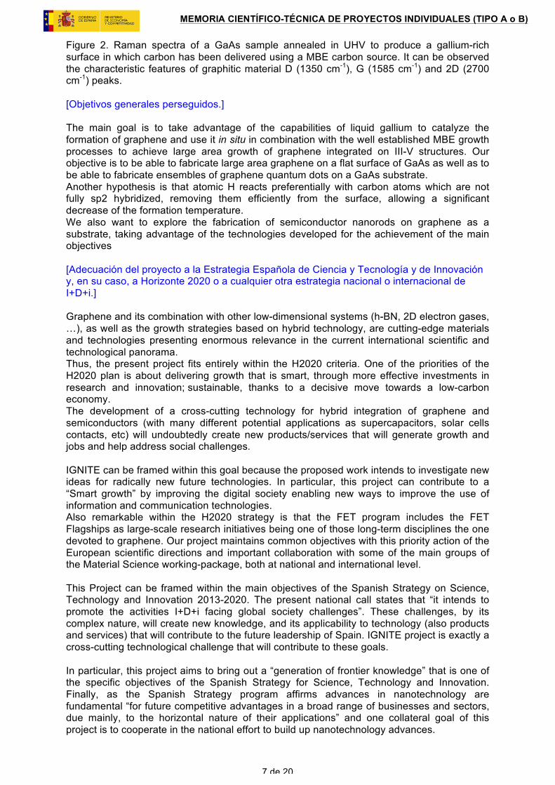
Figure 1. (a) Raman spectra of graphene grown on a Ga macroscopic droplet. These spectra are characteristic of high quality single layer graphene and demonstrate the excellent catalytic properties of gallium to synthesize graphene at 500ºC. (b) Synthesis of graphene on a macroscopic Ga droplet in an MBE using CBr4 as a carbon source at 400ºC. In figure 2, it can be observed very preliminary results obtained by Javier Mendez (ESISNA group) at Instituto de Ciencia de Materiales de Madrid (CSIC) in which a GaAs (001) sample has been annealed in Ultra High Vacuum to 720ºC to produce a gallium rich surface. This procedure has been done in a very uncontrolled way, because the experimental set up is designed for UHV STM and LEED characterization and does not have the capabilities required for in situ control of the surface of the semiconductor. Then, using a MBE carbon source that was designed and installed in their system under National Project REOMS- Reactividad de Moléculas Orgánicas en Superficies (MAT2011-26534), some atomic carbon has been delivered onto the semiconductor surface. Remarkably, the Raman spectra shows characteristic features of sp2 hybridized graphitic material. Also, recently, it has been reported the epitaxial growth of single-domain graphene on h-BN by a plasma-assisted Chemical Vapor Deposition (CVD) method. Large-area graphene single crystals were successfully grown for the first time on h-BN with a fixed stacking orientation. Epitaxial growth of graphene on h-BN was realized at a low temperature (500ºC) through a remote plasma-enhanced CVD (R-PECVD) process in which hydrogen plasma is believed to play a crucial role in the growth. Therefore, this project also proposes to explore the possibility of lowering the temperature for the growth of graphene on GaAs using atomic hydrogen. The hypothesis is that atomic H reacts preferentially with carbon atoms which are not fully sp2 hybridized. As a result, non graphitic material will form volatile CH4 chemical species. Therefore, amorphous carbon will be removed more effectively than graphene, leading to high quality graphene layers on GaAs produced at lower temperatures.
7 de 20
MEMORIA CIENTÍFICO-TÉCNICA DE PROYECTOS INDIVIDUALES (TIPO A o B)
Figure 2. Raman spectra of a GaAs sample annealed in UHV to produce a gallium-rich surface in which carbon has been delivered using a MBE carbon source. It can be observed the characteristic features of graphitic material D (1350 cm-1), G (1585 cm-1) and 2D (2700 cm-1) peaks. [Objetivos generales perseguidos.] The main goal is to take advantage of the capabilities of liquid gallium to catalyze the formation of graphene and use it in situ in combination with the well established MBE growth processes to achieve large area growth of graphene integrated on III-V structures. Our objective is to be able to fabricate large area graphene on a flat surface of GaAs as well as to be able to fabricate ensembles of graphene quantum dots on a GaAs substrate. Another hypothesis is that atomic H reacts preferentially with carbon atoms which are not fully sp2 hybridized, removing them efficiently from the surface, allowing a significant decrease of the formation temperature. We also want to explore the fabrication of semiconductor nanorods on graphene as a substrate, taking advantage of the technologies developed for the achievement of the main objectives [Adecuación del proyecto a la Estrategia Española de Ciencia y Tecnología y de Innovación y, en su caso, a Horizonte 2020 o a cualquier otra estrategia nacional o internacional de I+D+i.] Graphene and its combination with other low-dimensional systems (h-BN, 2D electron gases, …), as well as the growth strategies based on hybrid technology, are cutting-edge materials and technologies presenting enormous relevance in the current international scientific and technological panorama. Thus, the present project fits entirely within the H2020 criteria. One of the priorities of the H2020 plan is about delivering growth that is smart, through more effective investments in research and innovation; sustainable, thanks to a decisive move towards a low-carbon economy. The development of a cross-cutting technology for hybrid integration of graphene and semiconductors (with many different potential applications as supercapacitors, solar cells contacts, etc) will undoubtedly create new products/services that will generate growth and jobs and help address social challenges. IGNITE can be framed within this goal because the proposed work intends to investigate new ideas for radically new future technologies. In particular, this project can contribute to a “Smart growth” by improving the digital society enabling new ways to improve the use of information and communication technologies. Also remarkable within the H2020 strategy is that the FET program includes the FET Flagships as large-scale research initiatives being one of those long-term disciplines the one devoted to graphene. Our project maintains common objectives with this priority action of the European scientific directions and important collaboration with some of the main groups of the Material Science working-package, both at national and international level. This Project can be framed within the main objectives of the Spanish Strategy on Science, Technology and Innovation 2013-2020. The present national call states that “it intends to promote the activities I+D+i facing global society challenges”. These challenges, by its complex nature, will create new knowledge, and its applicability to technology (also products and services) that will contribute to the future leadership of Spain. IGNITE project is exactly a cross-cutting technological challenge that will contribute to these goals. In particular, this project aims to bring out a “generation of frontier knowledge” that is one of the specific objectives of the Spanish Strategy for Science, Technology and Innovation. Finally, as the Spanish Strategy program affirms advances in nanotechnology are fundamental “for future competitive advantages in a broad range of businesses and sectors, due mainly, to the horizontal nature of their applications” and one collateral goal of this project is to cooperate in the national effort to build up nanotechnology advances.

8 de 20
MEMORIA CIENTÍFICO-TÉCNICA DE PROYECTOS INDIVIDUALES (TIPO A o B)
The participant group is a well-recognized expert in his field. Thus we combine MBE growth, structural characterization, world-unique in situ characterization capabilities, optical and spectroscopic characterization and demonstrated cutting edge vacuum engineering, to step from fundamental science to application technology of new materials. [Los objetivos específicos, enumerándolos brevemente, con claridad, precisión y de manera realista (acorde con la duración prevista del proyecto). En los proyectos con dos investigadores principales, deberá indicarse expresamente de qué objetivos específicos se hará responsable cada uno de ellos.] We propose specific Objectives (O) that include several Work Packages (WP) as follows: O1. - Synthesis of graphene on III-V semiconductors. The possibility of integration of graphene together with III-V based heterostructures could lead to an innovative way of exploiting the combination of the exciting 2D properties of graphene with a mature optoelectronic technology like MBE. We will employ the catalytic properties of liquid Ga to synthesize graphene together with the integration of a carbon solid source cell into an III-V reactor. WP 1.1 Fabrication and installation of Carbon Cell
Task 1.1.1 Design and construction of a retractable carbon solid source compatible with the existing MBE processes. Task 1.1.2 Growth of Highly C-doped GaAs and electrical characterization Task 1.1.3 Growth of thick carbon layers and AFM measurements
Milestone1 (M1): fully operational C-cell WP 1.2. Preparation of Gallium rich surfaces
Task 1.2.1. Preparation of flat Ga-rich surfaces by MBE.
-In situ study of the surfaces reconstructions which are rich in gallium. -Ex situ characterization.
Task 1.2.2 Droplet epitaxy growths at substrate temperature compatible with graphene synthesis in GaAs (001) and GaAs (111) A substrates.
-Fabrication of gallium nanodroplets to be used as nucleation centers for the
synthesis of graphene nanostructures -Control of density, size and uniformity of Ga droplets
Task 1.2.3. Use of focused Ion Beam and/or Electron Beam Lithography for the fabrication of gallium nanostructures.
WP 1.3. Synthesis of graphene by evaporation of Carbon on Ga nanostructures.
Task 1.3.1. Synthesis of large area graphene on flat Ga-rich surfaces - Determination of the optimum growth conditions - Optical, electrical and/or structural characterization
Task 1.3.2. Synthesis of Graphene Quantum Dots on Ga droplets - Determination of the optimum growth conditions - Optical, electrical and/or structural characterization of nanostructures
Task 1.3.3. - Synthesis of Graphene on Ga nanostructures fabricated by FIB/EBL - Optical, electrical and/or structural characterization
9 de 20
MEMORIA CIENTÍFICO-TÉCNICA DE PROYECTOS INDIVIDUALES (TIPO A o B)
Milestone2 (M2): Detailed procedure for synthesis of graphene on GaAs. O2. - Growing G on GaAs at lower temperatures using atomic hydrogen The high temperatures required for catalytic reactions may prevent this technology to be compatible with standard III-V growth and processing methods. It would be very desirable to be able to grow graphene on GaAs at lower temperatures. With this aim we will study the role of atomic hydrogen in graphene synthesis. WP 2.1. Study of etching effects of H on graphene and other carbon deposits after growth WP 2.2. Study of modification of growth process of graphene under exposure to atomic H Milestone3 (M3): Realization of a technical document stating the feasibility and possible routes for using atomic H. O3. - Crystallization of gallium under arsenic in graphene on Ga Some of the envisioned applications will require removal of underlying Ga metal. This could be achieved by exposing the graphene synthesized on Ga to arsenic, with the aim of crystallization of Ga into a GaAs semiconductor matrix material. WP 3.1. Crystallization of liquid gallium under Graphene/Ga-rich surfaces: droplets & flat surfaces at high T. WP 3.2. Crystallization of liquid gallium under of Graphene/Ga-rich surfaces: droplets & flat surfaces at low T. Milestone4 (M4): Realization of a technical document stating the feasibility and possible routes to further proceed with removal of liquid Ga. O4. - Fabrication of GaAs/InAs nanorods on graphene layers as substrate The fabrication of active semiconductor nanostructures on graphitic-like substrates is considered as highly potential for flexible optoelectronics. Our aim is to produce nanorods on graphene layers grown by MBE in a monolithic process using a technology based on droplet epitaxy as for the growth of graphene layers by MBE. We will make this study in parallel on graphene layers grown by conventional methods. WP 4.1. Deposition of gallium and indium liquid droplets on graphene layers Task 4.1.1 Preparation of graphene on Si substrates for introduction in ultra-high vacuum environment. Task 4.1.2. Study of In/Ga droplet formation on graphene WP 4.2. Deposition of Ga and In liquid droplets on graphene grown by MBE WP 4.3. Growth of nanorods on graphene
Task 4.3.1 Study of the growth of nanorods on graphene assisted by In/Ga droplets seeds.
Task 4.3.2. Nanorods characterization by SEM Milestone5 (M5): Detailed procedure for growth of semiconductor nanorods on graphene [El detalle de la metodología propuesta, incluyendo la viabilidad metodológica de las tareas.] The proposed methodology is adapted to each specific Objective (O) with several Work Packages (WP) within as follows: O1.-Synthesis of graphene on dielectric and III-V semiconductors WP 1.1. Integration of a carbon solid source cell in one of the three existing III-V reactors The design of the cell will be done using advanced CAD programs using pre-existing models of the systems in which the cell will be incorporated. The calibration of the cell for high flux rates will be done by AFM profiling of sample in which very thick layers of carbon has been
10 de 20
MEMORIA CIENTÍFICO-TÉCNICA DE PROYECTOS INDIVIDUALES (TIPO A o B)
grown. The calibration of the cell for low flux rates will be done by Hall measurements of dopant density of carbon-doped GaAs. Carmen Robles will be in charge of fabrication and measurement of the devices. WP 1.2. Preparation of gallium-rich surfaces by MBE. The surface of GaAs samples will covered with gallium either by direct evaporation of Ga with a pre-existing Knudsen cell, or by thermal selective desorption of arsenic by annealing GaAs samples under very precisely controlled conditions. The surface will be characterized in situ by RHEED and Accumulated stress (Σσ) measurements. The surface morphology will be measured by AFM and SEM microscopes. The knowledge for preparation of high quality Ga-rich surfaces can be further transferred to other collaborators, for example to G*SURF project (MAT2014-54231-C4-1-P) in which the ESISNA group can perform STM and LEED characterization of samples prepared in their own experimental systems. We will explore also possibilities of using a Focused Ion Beam in collaboration with Dr. Daniel Granados to fabricated gallium nanostructures on different (h-BN, sapphire, HfO2, …) substrates that will be used in the next WP. WP 1.3. Synthesis of graphene by evaporation of carbon on gallium-rich MBE structures. Controlled amount of carbon will be delivered to the sample surface under various growth conditions. The surface will be characterized in situ by RHEED and Accumulated stress (Σσ) measurements. The surface morphology will be measured by AFM and SEM microscopes with the help of Raquel Alvaro. A key step of this WP is the ex situ characterization of the graphene by Raman and micro-Raman spectroscopy. This part of the WP will be done at IMM but it also can strongly interact with other external collaborators as Prof. Aron Pinczuk (University of Columbia iin the city of New York), Dra. Annette Plaut (Exeter University), and Dra. Nuria Garro Diaz & Dra. Ana Cros Stotter (University of Valencia). O2. - Growing graphene on GaAs at lower temperatures using atomic hydrogen WP 2.1. After growth treatments After synthesis of graphene on liquid Ga, the quality of the graphene layers will be determined by Raman spectroscopy. Surface morphology will be determined by AFM and SEM microscope with the help of Raquel Alvaro. This information will be used to improve the results and find optimum conditions for high quality graphene growth. WP 2.1. During-growth treatments. The quality of the surface will be characterized in real time and in situ by RHEED and accumulated stress (Σσ) measurements. Surface morphology will be determined by AFM and SEM microscope with the help of Raquel Alvaro. The quality of the graphene layers will be determined after synthesis by Raman spectroscopy. O3. - Crystallization of gallium with arsenic The process of crystallization of gallium will be explored by exposing graphene on GaAs to various arsenic fluxes at a wide range of temperatures. Surface morphology will be determined by AFM and SEM microscope. We will explore the crystallization process in (001) and (111) crystallographic GaAs orientations. O4. - Growing GaAs/InAs nanorods on graphene layers as substrate WP 4.1. Deposition of gallium and indium liquid droplets on graphene layers Firstly, we will develop a process for transferring graphene layers produced by conventional methods to a Si(111) substrate and introduce them into the MBE growth chamber. We will study (growth and characterization) the deposition of In and Ga metallic droplets on graphene to establish the experimental conditions for metallic droplet formation and control of size and density. The as-grown layers will be ex situ characterized by AFM and with the help of Raquel Álvaro.
11 de 20
MEMORIA CIENTÍFICO-TÉCNICA DE PROYECTOS INDIVIDUALES (TIPO A o B)
WP 4.2. Deposition of gallium and indium liquid droplets on graphene grown by MBE After the experience obtained in WP 4.1, we will study (growth and characterization) the In/Ga droplet formation process on MBE grown graphene layers. WP.4.3. Growth of nanorods on graphene Once controlled the Ga/In droplet formation on graphene substrates, we will proceed with the growth of nanorods by the well- established vapor-liquid-solid process. As Si(111) substrates are the most used for III-V nanorod fabrication, we will start extending the experimental conditions for nanorod nucleation on these substrates to graphene layers. The layers will be characterized by SEM with the help of Raquel Álvaro.. [Si fuera necesario, también se incluirá una evaluación crítica de las posibles dificultades de un objetivo específico y un plan de contingencia para resolverlas.] Although recent work suggest that gallium acts as a catalyst for graphene formation, it is not clear that under vacuum conditions and using a solid source of carbon the same results will be achieved. Without a doubt, the study of the synthesis of graphene under MBE-environment will provide a very useful knowledge. In any case we have a contingency plan for an alternative route just for the case that the graphene can not be synthesized under MBE conditions. Our plan would be the use of a combination of preparation of Ga rich structures by MBE and the use of Chemical Vapor Deposition for the synthesis of graphene on many other substrates as h-BN, Sapphire, HfO2, etc... The CVD growth on Ga-rich surfaces is in itself a very interesting route of exploration. It could be realize in the MBE reactor, or ex situ. Due to the extreme resilience of graphene against temperature treatments, ex situ synthesis of graphene by CVD could be further loaded into the MBE rector and cleaned to carry out further arsenization or capping process studies. [La descripción de los medios materiales, infraestructuras y equipamientos singulares a disposición del proyecto que permitan abordar la metodología propuesta.] The IMM will contribute with three fully operative Molecular Beam Epitaxy (MBE) reactors (figure 3 and figure 4) in which growths and in situ characterization by Reflection High Energy Diffraction (RHEED) and accumulated stress (Σσ) measurements will be carried out. A comprehensive list of the equipment available for this project can be found in our web page: http://www.imm-cnm.csic.es/mbe/inicio.php?page=laboratorios
12 de 20
MEMORIA CIENTÍFICO-TÉCNICA DE PROYECTOS INDIVIDUALES (TIPO A o B)
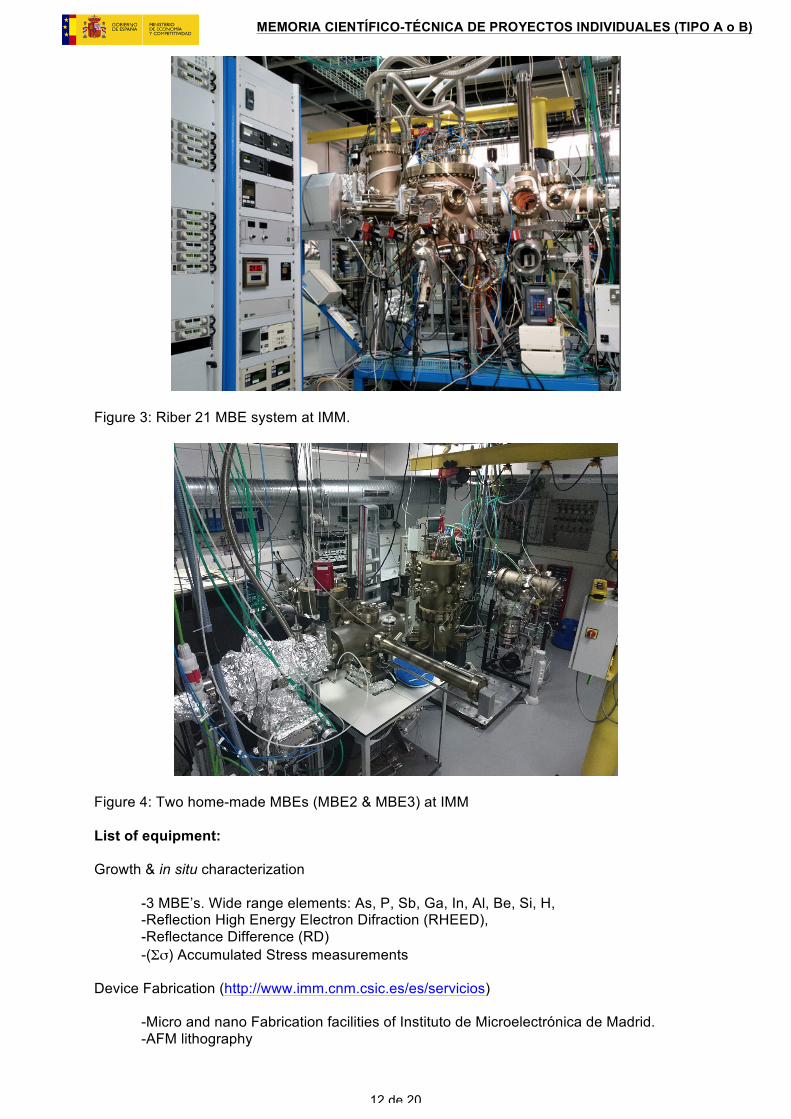
Figure 3: Riber 21 MBE system at IMM.
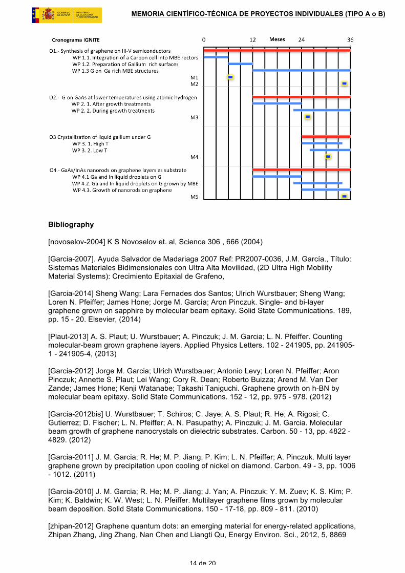
Figure 4: Two home-made MBEs (MBE2 & MBE3) at IMM List of equipment: Growth & in situ characterization
-3 MBE’s. Wide range elements: As, P, Sb, Ga, In, Al, Be, Si, H, -Reflection High Energy Electron Difraction (RHEED), -Reflectance Difference (RD) -(Σσ) Accumulated Stress measurements
Device Fabrication (http://www.imm.cnm.csic.es/es/servicios)
-Micro and nano Fabrication facilities of Instituto de Microelectrónica de Madrid. -AFM lithography

13 de 20
MEMORIA CIENTÍFICO-TÉCNICA DE PROYECTOS INDIVIDUALES (TIPO A o B)
-Electron Beam Lithography -Focused Ion Beam lithography
Optical Characterization
-Micro-Raman microscope with 532nm and 633 nm excitation laser. -Photoluminescence (PL) and confocal µPL at low temperatures (370-2300 nm, 4.2-300 K).
Structural Characterization
-AFM and Kelvin probe AFM -High Resolution Secondary Electron Microscope (SEM) FEI VERIOS 460 -SEM Zeiss LEO 145
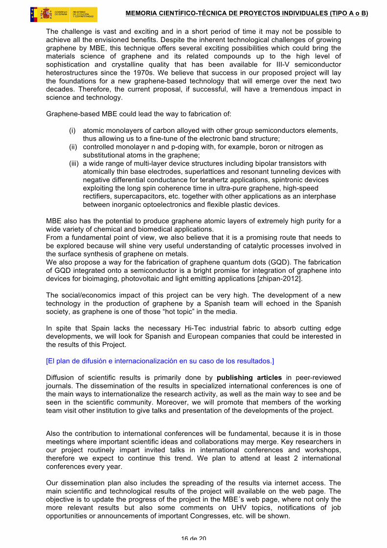
Also available for the project will be several Atomic Force Microscope for characterization of the surface morphology. A Scanning Probe Microscopy laboratory (Nanotec Electrónica S.L.) equipped with an optical microscope (10 micron resolution) with CCD, oscilloscope, second dynamic board for Kelvin Probe Force Measurements and Conductive Atomic Force Microscopy with current sensibility down to the pico-Ampere range. The system is mounted on an anti-vibrational table, shielded by a grounded Faraday cage. The sample is held in controlled atmosphere (N2,dry air, etc) and can be locally illuminated with a tunable source for surface photovoltage measurements. A micro Raman microscope with 532nm and 633 nm excitation laser lines for characterization of the quality of graphene and a magnetoluminescence lab for optical characterization. The Micro- and Nano- Fabrication (MiNa) services (www.imm.cnm.csic.es/en/servicios) of the Instituto de Microelectrónica de Madrid will be available for processing contacts on the samples for their electrical characterization. We will use two Scanning Electron Microscope (SEM) available at IMM. One of the equipment is a Zeiss (LEO 145) that will be used for electron lithography for the fabrication of gallium structures on the surface. Particularly relevant for this project is the availability of a new High Resolution Secondary Scanning Electron Microscope (SEM) that will be installed at the Instituto de Microelectronica de Madrid in 2015. The equipment is a FEI Verios 460 with 0.6 nm resolution at 15KeV and 0.7 nm resolution at 1KeV. It also has compositional contrast, cristalographic analysis capabilities. This equipment is crucial for the characterization of the droplet epitaxial nanostructures that we propose to fabricate. It will also provide a fast, accurate characterization of the graphene layers grown on the samples. [Un cronograma claro y preciso de las fases e hitos previstos en relación con los objetivos planteados en la propuesta.] Cronograma
14 de 20
MEMORIA CIENTÍFICO-TÉCNICA DE PROYECTOS INDIVIDUALES (TIPO A o B)
Bibliography [novoselov-2004] K S Novoselov et. al, Science 306 , 666 (2004) [Garcia-2007]. Ayuda Salvador de Madariaga 2007 Ref: PR2007-0036, J.M. García., Título: Sistemas Materiales Bidimensionales con Ultra Alta Movilidad, (2D Ultra High Mobility Material Systems): Crecimiento Epitaxial de Grafeno, [Garcia-2014] Sheng Wang; Lara Fernades dos Santos; Ulrich Wurstbauer; Sheng Wang; Loren N. Pfeiffer; James Hone; Jorge M. García; Aron Pinczuk. Single- and bi-layer graphene grown on sapphire by molecular beam epitaxy. Solid State Communications. 189, pp. 15 - 20. Elsevier, (2014) [Plaut-2013] A. S. Plaut; U. Wurstbauer; A. Pinczuk; J. M. Garcia; L. N. Pfeiffer. Counting molecular-beam grown graphene layers. Applied Physics Letters. 102 - 241905, pp. 241905-1 - 241905-4, (2013) [Garcia-2012] Jorge M. Garcia; Ulrich Wurstbauer; Antonio Levy; Loren N. Pfeiffer; Aron Pinczuk; Annette S. Plaut; Lei Wang; Cory R. Dean; Roberto Buizza; Arend M. Van Der Zande; James Hone; Kenji Watanabe; Takashi Taniguchi. Graphene growth on h-BN by molecular beam epitaxy. Solid State Communications. 152 - 12, pp. 975 - 978. (2012) [Garcia-2012bis] U. Wurstbauer; T. Schiros; C. Jaye; A. S. Plaut; R. He; A. Rigosi; C. Gutierrez; D. Fischer; L. N. Pfeiffer; A. N. Pasupathy; A. Pinczuk; J. M. Garcia. Molecular beam growth of graphene nanocrystals on dielectric substrates. Carbon. 50 - 13, pp. 4822 - 4829. (2012) [Garcia-2011] J. M. Garcia; R. He; M. P. Jiang; P. Kim; L. N. Pfeiffer; A. Pinczuk. Multi layer graphene grown by precipitation upon cooling of nickel on diamond. Carbon. 49 - 3, pp. 1006 - 1012. (2011) [Garcia-2010] J. M. Garcia; R. He; M. P. Jiang; J. Yan; A. Pinczuk; Y. M. Zuev; K. S. Kim; P. Kim; K. Baldwin; K. W. West; L. N. Pfeiffer. Multilayer graphene films grown by molecular beam deposition. Solid State Communications. 150 - 17-18, pp. 809 - 811. (2010) [zhipan-2012] Graphene quantum dots: an emerging material for energy-related applications, Zhipan Zhang, Jing Zhang, Nan Chen and Liangti Qu, Energy Environ. Sci., 2012, 5, 8869

15 de 20
MEMORIA CIENTÍFICO-TÉCNICA DE PROYECTOS INDIVIDUALES (TIPO A o B)
[lippert-2011] G Lippert et. al, Phys. Stat. Solidi B 248 , 2619 (2011) [Lzhang-2012] L. C. Zhang et al. Vapour-phase graphene epitaxy at low temperatures. Nano Res. 5, 258_264 (2012) [ding-2013] Chemical vapor deposition of graphene on liquid metal catalysts, G. Ding et al. Carbon 53 (2013) 321. [yang-2013] Epitaxial growth of single-domain graphene on hexagonal boron nitride, W. Yang et al., Net. Mat. 12, 792 (2013) [wang-2013] High-mobility graphene on liquid p-block elements by ultra-low-loss CVD growth, J. Wang et al., Scientific Reports, 3, 2670, (2013). [Alonso-González-2007] Formation and optical characterization of single InAs quantum dots grown on GaAs nanoholes, Appl.Phys. Lett. 91 (2007) 163104. [Chul_Ho Lee -2011]. Flexible Inorganic Nanostructure Light-Emitting Diodes Fabricated on Graphene Films Adv. Mat. 25, 4614 (2011) [J.Mendez 2014] Irene Hernández-Rodríguez; Jorge M. Garcia; José A. Martín-Gago; Pedro L. de Andrés; Javier Méndez.Graphene growth on Pt(111) and Au(111) using a MBE carbon solid-source. Diamond and Related Materials. Elsevier, 05/03/2015. <http://dx.doi.org/10.1016/j.diamond.2015.03.004>. [Garcia-2014bis] Jorge M. García; Benito Alen; Juan P. Silveira; Daniel Granados, (2014), 0D Band Gap Engineering by MBE Quantum Rings: Fabrication and optical properties. Physics of Quantum Rings. Springer, Fomin, Vladimir, (Ed.), 31/08/2013. ISBN 978-3-642-39196-5 [Alonso-Gonzalez 2008] Low density InAs quantum dots with control in energy emission and top surface location. Appl. Phys. Lett. 93, 183106 (2008) [Alonso-Gonzalez 2009] Formation of Lateral Low Density In(Ga)As Quantum Dot Pairs in GaAs Nanoholes, Crystal Growth & Design 9 (2009) 2525 [Fuster 2014] Fundamental role of arsenic flux in nanohole formation by Ga droplet etching on GaAs(001). Nan. Res. Lett. 9, 309 (2014). C.2. IMPACTO ESPERADO DE LOS RESULTADOS [Descripción del impacto científico-técnico social y/o económico que se espera de los resultados del proyecto, tanto a nivel nacional como internacional.] The synthesis of graphene by MBE has been a challenge since the early discovery of its amazing properties. Growing graphene by MBE could lead to many benefits that have been already envisioned since early 2007. Among many advantages, the one that emerges as the most predominant is the possibility of synthesizing high quality large-area graphene on a flat surface, with control of its electric doping. Many MBE labs with a carbon source have tried since then the growth of high quality graphene. As an example, the group leaded by Dr. Sergei Novikov, Prof. C. Thomas Foxon and Prof. Laurence Eaves at the University of Nottingham, UK is putting together two dedicated new MBE systems for this purpose investing more than two million pounds. Their chosen route is the use of very high temperatures during growth of G on h-BN substrates. From our point of view, even though many useful applications could be find for that approach, the true technological challenge is the synthesis and integration of graphene with the state-of-the-art optoelectronic material: GaAs and related compounds.
16 de 20
MEMORIA CIENTÍFICO-TÉCNICA DE PROYECTOS INDIVIDUALES (TIPO A o B)
The challenge is vast and exciting and in a short period of time it may not be possible to achieve all the envisioned benefits. Despite the inherent technological challenges of growing graphene by MBE, this technique offers several exciting possibilities which could bring the materials science of graphene and its related compounds up to the high level of sophistication and crystalline quality that has been available for III-V semiconductor heterostructures since the 1970s. We believe that success in our proposed project will lay the foundations for a new graphene-based technology that will emerge over the next two decades. Therefore, the current proposal, if successful, will have a tremendous impact in science and technology. Graphene-based MBE could lead the way to fabrication of:
(i) atomic monolayers of carbon alloyed with other group semiconductors elements, thus allowing us to a fine-tune of the electronic band structure;
(ii) controlled monolayer n and p-doping with, for example, boron or nitrogen as substitutional atoms in the graphene;
(iii) a wide range of multi-layer device structures including bipolar transistors with atomically thin base electrodes, superlattices and resonant tunneling devices with negative differential conductance for terahertz applications, spintronic devices exploiting the long spin coherence time in ultra-pure graphene, high-speed rectifiers, supercapacitors, etc. together with other applications as an interphase between inorganic optoelectronics and flexible plastic devices.
MBE also has the potential to produce graphene atomic layers of extremely high purity for a wide variety of chemical and biomedical applications. From a fundamental point of view, we also believe that it is a promising route that needs to be explored because will shine very useful understanding of catalytic processes involved in the surface synthesis of graphene on metals. We also propose a way for the fabrication of graphene quantum dots (GQD). The fabrication of GQD integrated onto a semiconductor is a bright promise for integration of graphene into devices for bioimaging, photovoltaic and light emitting applications [zhipan-2012]. The social/economics impact of this project can be very high. The development of a new technology in the production of graphene by a Spanish team will echoed in the Spanish society, as graphene is one of those “hot topic” in the media. In spite that Spain lacks the necessary Hi-Tec industrial fabric to absorb cutting edge developments, we will look for Spanish and European companies that could be interested in the results of this Project. [El plan de difusión e internacionalización en su caso de los resultados.] Diffusion of scientific results is primarily done by publishing articles in peer-reviewed journals. The dissemination of the results in specialized international conferences is one of the main ways to internationalize the research activity, as well as the main way to see and be seen in the scientific community. Moreover, we will promote that members of the working team visit other institution to give talks and presentation of the developments of the project.
Also the contribution to international conferences will be fundamental, because it is in those meetings where important scientific ideas and collaborations may merge. Key researchers in our project routinely impart invited talks in international conferences and workshops, therefore we expect to continue this trend. We plan to attend at least 2 international conferences every year. Our dissemination plan also includes the spreading of the results via internet access. The main scientific and technological results of the project will available on the web page. The objective is to update the progress of the project in the MBE´s web page, where not only the more relevant results but also some comments on UHV topics, notifications of job opportunities or announcements of important Congresses, etc. will be shown.
17 de 20
MEMORIA CIENTÍFICO-TÉCNICA DE PROYECTOS INDIVIDUALES (TIPO A o B)
Finally, all the participants into the project feel a strong commitment with outreach for the general public. Thus, we will continue imparting lectures in secondary school, showing our laboratories, or writing articles in national newspapers for the general public. We are also members of the network NANODYF, http://www.nanodyf.org/, coordinated by Dr. Joaquin Dario Tutor Sanchez that intends to divulge the nanoscience and nanotechnology culture. This platform will be used to disseminate our results. [Si se considera que puede haber transferencia de resultados, se deberán identificar los resultados potencialmente transferibles y detallar el plan previsto para la transferencia de los mismos.] The group has applied for three patents related to the fabrication of graphene in the past, and we have some patents with international extension (PCT). Many of the results that may be produced in IGNITE project are sensitive to be protected via patents. If the concepts and hypothesis are valid, we expect to be able to patent around month 30 of the workplan a procedure for hybid integration of graphene in GaAs. We could also protect intellectual knowledge related to the fabrication of ensembles of graphene quantum dots with controlled size, aprox. by the end of the project. The carbon evaporation technology is already patented. We will contact CSIC Deputy Vice-Presidency for Knowledge Transfer (VATC, Vicepresidencia Adjunta de Transferencia del Conocimiento) to speed up the process of protecting the results of our research by means of a patent or a utility model. We will get VATC help us to work with possible companies interested in presenting a joint proposal to a public call for expressions of interest. We plan to receive also from VATC technology service (analysis, tests, validations) and to obtain consultancy services. We also plan to look for the help professional team to speed up writing and proceeding with all the details involved in patenting. C.3. CAPACIDAD FORMATIVA DEL EQUIPO SOLICITANTE [El plan de formación previsto en el contexto del proyecto solicitado.] The training of the graduate student linked to this proposal will mainly rely on the research and will be involved in all the workpackages, under the supervision of the PhD thesis advisor. Given the range of activities, from growth developments to advanced experiments and design and fabrication of novel epitaxial structures, the project will provide a comprehensive, multifaceted exposure to the student, who will have the opportunity to acquire a very broad education. The scope of the challenges faced in IGNITE project are suitable for the training of young scientists. Frequent meetings with collaborators, where the research plans, problems and advancements will be discussed openly, will take place and the active participation of the students will be encouraged. Given the close collaboration with the project G*SURF MINECO Project (Ref. MAT2014-54231-C4-1-P), we plan visits of the students to the labs of those research labs and have discussions with other students to foster collaborative attitude among the students and strengthen the collaborative links between partners. During the thesis period, the students participate in university doctoral programs. For the students to also acquire presentation skills, they will be required to give oral presentations of their results at meetings and to submit papers for oral talks at international conferences. This will be complemented with publication writing skills that will be obtained by close interaction with their mentors in the process of wrapping up the research results and sending them for publication. The students will be encouraged to receive the specific training courses organized by “Gabinete de Formación del CSIC” on writing and speaking English. As an essential complement to their education, our students will be encouraged to use the “Estancias en el extranjero” programs of different kind of scholarships to expend a few
18 de 20
MEMORIA CIENTÍFICO-TÉCNICA DE PROYECTOS INDIVIDUALES (TIPO A o B)
months per year in research stays in first class groups abroad. This practice has given excellent results with our former PhD students. Our student will also have be trained working within the ISO 9001 quality standard certification in our Micro and Nano Fabrication Facilities. The MBE team is extremely experienced in supervising PhD thesis. The MBE group have successfully supervised more than 11 PhD students during the last 10 years. The MBE group has a long experience in the training of young researchers. In the past the students mentored by MBE group has reached outstanding positions as can be observed next. Remarkably, our students has joined top level research groups in USA, Europe as well as some of them have been hired by High Tech national and international companies (ISOFOTON, Thales-Alenia, Camlin Technologies, Solar Junction). Dr. Pablo Alonso has recived a recognition awards “premio de Física de la Real Sociedad Española de Física (RSEF)-Fundación BBVA 2014, Investigadores Noveles de Física Experimental”. Dr. Daniel Granados is currently Director of the IMDEA nanociencia fabrication facilities. Dr. Ferran Suarez has contribute with his work at Solar Junction in 2013 to achieve a triple-junction Solar Cell efficiency (44.1%) record in 2014 (http://www.iqep.com/news/2013/08/solar-junction/).
[Relación de tesis realizadas o en curso (últimos 10 años) con indicación del nombre del doctorando, el título de tesis y la fecha de obtención del grado de doctor o de la fecha prevista de lectura de tesis. Breve descripción del desarrollo científico o profesional de los doctores egresados del equipo de investigación.] During the last years, our laboratory has received and trained successfully Ph.D. within the FPI programme. Our training capacity is supported by a number of doctoral thesis performed in our laboratories. On going Doctoral thesis: -Andrés Raya, 2018, “Nanoestructuras embebidas en nanohilos semiconductores epitaxiales para células solares”, Supervisor: David Fuster, Jose M Llorens -Lukasz Wevior, 2015, “Optical investigation of spin and charge interactions in single semiconductor quantum dots”, Supervisor: Benito Alen -Jesús Iván Zamorano, 2015, Fabricación y caracterización de nanoestructuras con orden lateral, tamaño homogéneo y control en densidad para su aplicación en dispositivos optoelectrónicos y fotónicos¨, Supervisor: Yolanda González Doctoral thesis in the last 10 years in MBE group at IMM: -Iván Prieto González, 2014, Design, fabrication and characterization of photonic crystals for cavity quantum electrodynamics enhanced devices. Co-supervised by: Aitor Postigo, Yolanda González. Actual position: Research contract at universidad ETH (Zurich) in the group of Prof. Bertram Batlogg. -Diego Alonso Álvarez, 2011, "Strain balanced epitaxial stacks of quantum dots and posts". Co-supervised by: Benito Alén, José María Ripalda Cobián. Actual position: Marie-Curie fellowship at Imperial College, Londres (UK). -Alfonso González Taboada, 2010, "Control de la forma, tamaño y composición de nanoestructuras de semiconductores III-V: anillos y puntos cuánticos". Co-supervised by: José María Ripalda Cobián, Jorge M. García. Actual position: Camlin Technologies (http://www.camlintechnologies.com/research.php) research team, Zurich, Switzerland. Responsible for MBE growths. -Guillermo Muñoz Matutano, 2010, "Excitones y triones en nanoestructructuras semiconductoras de InAs". Co-supervised by: Benito Alén, Juan Mtnez. Pastor .
19 de 20
MEMORIA CIENTÍFICO-TÉCNICA DE PROYECTOS INDIVIDUALES (TIPO A o B)
Actual position: Juan de la Cierva research contract at Universidad Politécnica de Valencia. -Luis Javier Martínez Rodríguez, 2009, "Design, fabrication and characterization of photonic crystals on III-V compounds: from classical to quantum light sources", Supervisor by: Pablo Aitor Postigo Resa. Actual position: Investigador del Centre National de la Recherche Scientifique (CNRS), Orsay Cedex, Francia -Javier Martín Sánchez, 2009, “Crecimiento selectivo de InAs sobre substratos grabados de GaAs(001) mediante litografia de oxidacion local por AFM" (2009), Supervisor: Yolanda González. Actual position: Research contract at Johannes Kepler Universität (Austria), Group of Prof. Armando Rastelli. -Pablo Alonso González, 2009, "Formation of ordered III-V semiconductor nanostructures by different technological approaches" (2009), Supervisor: Luisa González Sotos. Actual position: Post-doctoral Researcher, Nanooptics Group, nanoGUNE. -Ferrán Suarez González, 2009, "Aspectos de crecimiento, fabricación y caracterización de diodos láser basados en nanoestructuras semiconductoras" (2007) Supervisor:: Mª Luisa Dotor. Actual position: Research Contract at Solar Junction (http://www.sj-solar.com/), San Diego California, EEUU. -Alfonso Rodriguez Alija, 2007, Fabricación de nanoestructuras semiconductoras con banda prohibida para fotones y su aplicación a dispositivos optoelectrónicos integrados" (2007) Supervisor: Pablo Aitor Postigo. Actual position: Research contract at Thales-Alenia (Tres Cantos). -Daniel Granados Ruiz, 2006, "Nanoestructuras auto-ensambladas mediante epitaxia por haces moleculares de InAs sobre substratos de GaAs(001): de los puntos a los anillos cuánticos" (2006). Supervisor: Jorge M. García. Actual position: Director of Nanofabrication Cleanroom facilities at IMDEA nanociencia. Ramón y Cajal Grant. -David Fuster Signes, 2006, "Crecimiento y caracterización de hilos cuánticos auto-ensamblados de arseniuro de indio sobre substratos de fosfuro de indio", Co-supervised by: Luisa González Sotos (IMM), Juan Martínez Pastor (ICMUV). Actual position: Research contract at IMM, CNM-CSIC. C.4. IMPLICACIONES ÉTICAS Y/O DE BIOSEGURIDAD There are no expected ethical or biosecurity-related implications.