desarrollo de una unidad de control para un sistema de...
TRANSCRIPT

UNIVERSIDAD DE VALLADOLID
ESCUELA DE INGENIERIAS INDUSTRIALES
Máster en Ingeniería Industrial
Desarrollo de una unidad de control para un
sistema de ignición de superficie caliente
usado en motores de combustión interna.
Autor:
Del Río Carbajo, Mario
Blanca Giménez Olavarría
Hochschule Karlsruhe
Valladolid, Junio 2016.

TFM REALIZADO EN PROGRAMA DE INTERCAMBIO
TÍTULO: Development of a fast-acting control unit for a hot surface ignition
system used in internal combustion engines
ALUMNO: Mario del Río Carbajo
FECHA: 30/03/2016
CENTRO: Hochschule Karlsruhe - Technik und Wirtschaft
TUTOR: Prof. Dr.-Ing. Maurice Kettner

Resumen
Un nuevo Sistema de ignición para motores estacionarios ha sido desarrollado. Consiste en el
uso de una bujía incandescente que se comporta como una resistencia PTC. La temperatura de
la bujía incandescente es la encargada de regular el comienzo de la combustión, por ello es
necesario efectuar un control preciso sobre su temperatura.
En este proyecto, un nuevo controlador es diseñado y construido, intentando mejorar el
rendimiento del anterior. Para la programación del controlador se usara un microcontrolador.
Además se construirá un circuito para el procesamiento de señales, de tal forma que el
controlador pueda funcionar independientemente, requiriendo solamente el uso de la fuente
de alimentación correspondiente.
Se cree que este sistema puede mejorar la relación ente eficiencia y emisiones de NOx ,
además de reducir los costes de mantenimiento. Pero en primer lugar, se necesita un
controlador que sea capaz de mantener la temperatura de la bujía constante.
Palabras claves
Controlador de temperatura, motor de gas natural, Arduino, procesamiento de señales y
sistema de ignición.


Master’s Thesis
Development of a Fast-Acting Control
Unit for a Hot Surface Ignition System
Used in Internal Combustion Engines
Winter Semester 2015/16
Student:
Mario del Río Carbajo, Matr.-Nr.:54949
Supervisor Hochschule Karlsruhe:
Prof. Dr.-Ing. Maurice Kettner
Supervisor IKKU:
Fino Scholl, M. Sc.
Engine Technology Research Group of the Institute of Refrigeration, Air Condi-
tioning and Environmental Engineering (IKKU)


III
Task of Thesis
A new ignition system, which works in stationary Natural Gas engines, has been developed.
This new system uses a glow plug, whose behaviour is like a PTC resistor and thus its re-
sistance has a relationship with its temperature. This temperature enables adjust the start of
combustion, therefore a control over this temperature is totally necessary with the purpose of
selecting when the combustion starts.
In this thesis, a new controller is built, trying to improve the performance of the previous one.
One of the goals to be improved is to operate the controller at bigger frequencies, allowing for
a faster correction of the error. The controller will be programed using a microcontroller, and
the circuit, which the microcontroller requires, will be built with the aim of operating this new
controller with the only necessity of the external power supply.
It is believed that this new system can improve the trade-off between efficiency and NOx
emissions. Furthermore, the maintenance costs will be reduced. But first of all, a controller,
which will able to keep the temperature steady, is necessary in order to reduce the cycle to
cycle variation.


V
Declaration of Originality
I hereby declare that this thesis and the work reported herein was composed by and originated
entirely from me. Information derived from the published and unpublished work of others has
been acknowledged in the text and references are given in the list of sources.
Place and Date Signature
Mario del Río Carbajo


VII
Acknowledgments
I would like to offer my sincerest gratitude to my supervisor in the Hochschule Karlsruhe,
Prof. Dr.-Ing. Maurice Kettner, and my supervisor at the IKKU, Fino Scholl, M. Sc., for their
help and continued assistance throughout the whole development of this master’s thesis.
I would like to thank all the personal of the Hoschule Karlruhe who have helped me during
this time. I give a special thanks to Mr. Forstner for his special help in the building process of
the circuit.
I would like to acknowledge with gratitude to Lourdes Alonso Hernández her help with the
report's correction.
I also thank my tutor at the University of Valladolid, Dr. Blanca Giménez Olavarría, for mak-
ing possible this experience and for her support.
I dedicate a special gratitude to my family and my girlfriend Belén, who have always support-
ed me with their trust, love and sacrifice.
Karlsruhe, April 2016 Mario del Río Carbajo


IX
Index
Task of Thesis .......................................................................................................................... III
Declaration of Originality ......................................................................................................... V
Acknowledgments ................................................................................................................... VII
Index ......................................................................................................................................... IX
List of Abbreviations ................................................................................................................ XI
List of symbols ...................................................................................................................... XIII
1 Introduction ........................................................................................................................ 1
1.1 Goals of the Thesis ..................................................................................................... 3
1.2 Basic concept of the controller ................................................................................... 3
2 MATLAB and Simulink ..................................................................................................... 7
2.1 Brief description of the program ................................................................................ 7
2.2 Development of the program ...................................................................................... 8
2.3 Making tests with Simulink ...................................................................................... 10
2.3.1 Selecting values of the different parameters and running tests .......................... 10
2.3.2 Second part, writing data in an Excel file .......................................................... 11
2.4 Test trials .................................................................................................................. 12
2.4.1 Influence of new controller ................................................................................ 13
2.4.2 Conditions in the combustion chamber .............................................................. 15
3 Circuit design and its components ................................................................................... 19
3.1 Microcontroller ......................................................................................................... 19
3.2 Circuit for voltage measurement .............................................................................. 21
3.2.1 Circuit sensitivity ............................................................................................... 26
3.3 Circuit for current measurement .............................................................................. 28
3.3.1 Shunts ................................................................................................................. 28
3.3.2 Direct current current-transformer ..................................................................... 29
3.3.3 Open-loop Hall Effect current transducers ......................................................... 29
3.3.4 Closed-loop hall effect current sensors .............................................................. 30
3.3.5 Selection ............................................................................................................. 31
3.3.6 Scheme for the circuit ........................................................................................ 31
3.3.7 Circuit sensitivity ............................................................................................... 34
3.4 Digital Switch circuit ............................................................................................... 35
4 Components ...................................................................................................................... 39
4.1 Analog-to-digital converter (ADC) .......................................................................... 39
4.2 Liquid crystal display ............................................................................................... 42
4.3 Push button ............................................................................................................... 43
4.4 Precision programmable reference ........................................................................... 44
4.5 Operational amplifier ............................................................................................... 45

X Index
4.6 Noise considerations for the circuit design .............................................................. 46
5 Practical Testing ............................................................................................................... 49
5.1 Digital Switch circuit ............................................................................................... 49
5.2 Problem with the computer adapter ......................................................................... 54
5.3 Circuits for current and voltage measurement ......................................................... 56
5.4 Calibration of the circuits for current and voltage measurement ............................. 60
6 Programming Arduino ...................................................................................................... 63
6.1 Programming code ................................................................................................... 64
6.1.1 Beginning of the program .................................................................................. 64
6.1.2 Setup() ................................................................................................................ 65
6.1.3 Loop() ................................................................................................................. 66
7 Fast Adaptive Saturated (FAS) Controller ....................................................................... 67
7.1 Controller operation ................................................................................................. 67
7.2 Test of the controller working .................................................................................. 69
7.3 Response of the controller ........................................................................................ 72
8 Problem working with the engine .................................................................................... 75
9 Conclusion ........................................................................................................................ 77
Bibliography ............................................................................................................................. 79
Table of Figures ....................................................................................................................... 81
Appendix A: Programming code for Arduino .......................................................................... 85

XI
List of Abbreviations
Abbreviation Description
A Analog
AC Alternating Current
ADC Anolog-To-Digital Converter
CLK Clock
CPU Central Processing Unit
CS Chip Select
D Drain (terminal)
D Digital
DAC Digital-to-Analog Converter
DC Direct Current
DCCT Direct Current Current-Transformer
Din Data in
Dout Data out
EEPROM Electrically Erasable Programmable Read-Only Memory
FAS Fast Adaptive Saturated (controller)
G Gate (terminal)
GMR sensors Giant Magneto Resistance sensors
GND Ground
HIS Hot Surface Ignition
I/O Input(S)/Output(S)
I2C Inter-integrated Circuit
IC Integrated Circuit
IDE Integrated Development Environment
LCD Liquid Crystal Display
LSB Lest Significant Bit
MISO Master Input Slave Output
MOSI Master Output Slave Input
NOx Nitrogen Oxide
Op amp Operational amplifier
PID Proportional-Integral-Derivative Controller
PTC Positive Temperature Coefficient
PTC Positive Temperature Coefficient
PWM Pulse-Width Modulation
RAM Random Access Memory
REF Reference

XII List of abbreviations
ROM Read-Only Memory
S Source (terminal)
SAR Successive-Approximation Register
SCL Serial Clock Line
SDA Serial Data Line
SHA Sample-and-Hold Amplifier
SHDN Shutdown Input
SPI Serial Peripheral Interface
SS Select Signal
TTL Transistor-Transistor Logic
USB Universal Serial Bus
XIII
List of symbols
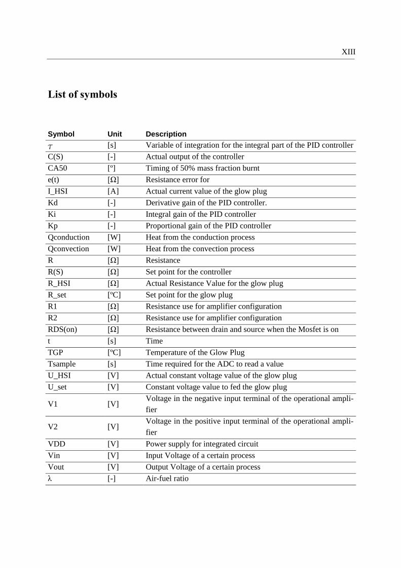
Symbol Unit Description
[s] Variable of integration for the integral part of the PID controller
C(S) [-] Actual output of the controller
CA50 [º] Timing of 50% mass fraction burnt
e(t) [Ω] Resistance error for
I_HSI [A] Actual current value of the glow plug
Kd [-] Derivative gain of the PID controller.
Ki [-] Integral gain of the PID controller
Kp [-] Proportional gain of the PID controller
Qconduction [W] Heat from the conduction process
Qconvection [W] Heat from the convection process
R [Ω] Resistance
R(S) [Ω] Set point for the controller
R_HSI [Ω] Actual Resistance Value for the glow plug
R_set [ºC] Set point for the glow plug
R1 [Ω] Resistance use for amplifier configuration
R2 [Ω] Resistance use for amplifier configuration
RDS(on) [Ω] Resistance between drain and source when the Mosfet is on
t [s] Time
TGP [ºC] Temperature of the Glow Plug
Tsample [s] Time required for the ADC to read a value
U_HSI [V] Actual constant voltage value of the glow plug
U_set [V] Constant voltage value to fed the glow plug
V1 [V] Voltage in the negative input terminal of the operational ampli-
fier
V2 [V] Voltage in the positive input terminal of the operational ampli-
fier
VDD [V] Power supply for integrated circuit
Vin [V] Input Voltage of a certain process
Vout [V] Output Voltage of a certain process
λ [-] Air-fuel ratio


1
1 Introduction
The conventional ignition system (spark ignition),which is used in natural gas engine, sets
restrictive limits regarding to the air-fuel relation and requires high level of maintenance due
to electrode wear. With the aim of solving this problem, a new ignition system has been de-
veloped. Due to its larger mixture volume, working with lower air-fuel ratio is possible. As a
consequence, the trade-off between engine efficiency and NOx is improved.
The solution for this system is based on the use of a glow plug, whose temperature is con-
trolled by a power supply working along with a PID controller. The glow plug consists of an
electrically conductive solid ceramic with PTC-behaviour, which it is depicted in Figure 1,
and thanks to its almost quadratic correlation between resistance and temperature, allows to
know its temperature by measuring the resistance.
Figure 1: Correlation Resistance-Temperature for the glow plug [1]
One of the keys for the good performance of this system is to keep this resistance value steady
while the engine is working. Previous experiments showed that by fixing the voltage value,
the glow plug was not able to keep its temperature steady. For this reason, a closed loop con-
troller is necessary.
A controller with this purpose was developed. In this controller the error was reduced by
modifying the voltage value of the power supply. This error was the difference between the
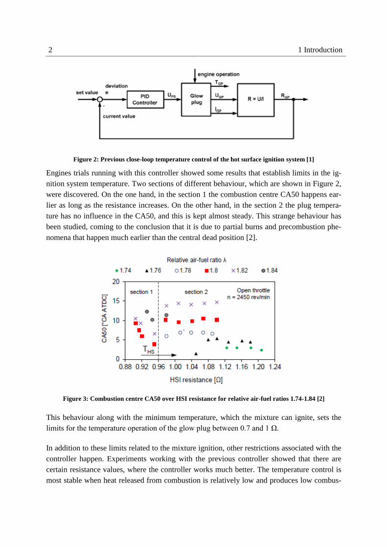
current value and the set point value, and it could be changed freely. A diagram where the
working principle of this controller is depicted appears in Figure 2.
y = 0.001x + 0.152R² = 0.999
0.2
0.3
0.4
0.5
0.6
0.7
0.8
0.9
200 400 600 800 1000 1200 1400
Resis
tan
ce R
HS
I[Ω
]
Hot surface temperature THS [ C]
2 1 Introduction
Figure 2: Previous close-loop temperature control of the hot surface ignition system [1]
Engines trials running with this controller showed some results that establish limits in the ig-
nition system temperature. Two sections of different behaviour, which are shown in Figure 2,
were discovered. On the one hand, in the section 1 the combustion centre CA50 happens ear-
lier as long as the resistance increases. On the other hand, in the section 2 the plug tempera-
ture has no influence in the CA50, and this is kept almost steady. This strange behaviour has
been studied, coming to the conclusion that it is due to partial burns and precombustion phe-
nomena that happen much earlier than the central dead position [2].
Figure 3: Combustion centre CA50 over HSI resistance for relative air-fuel ratios 1.74-1.84 [2]
This behaviour along with the minimum temperature, which the mixture can ignite, sets the
limits for the temperature operation of the glow plug between 0.7 and 1 Ω.
In addition to these limits related to the mixture ignition, other restrictions associated with the
controller happen. Experiments working with the previous controller showed that there are
certain resistance values, where the controller works much better. The temperature control is
most stable when heat released from combustion is relatively low and produces low combus-

1.1 Goals of the Thesis 3
tion temperatures. This happens when the engine works with high air-fuel ratios or advanced
combustion phasing.
Considering this behaviour, it can be said that perturbations have a big influence in the stabil-
ity of the controller. For this reason, the design of a new controller is necessary to open up the
operation conditions that are restricted for the current controller.
1.1 Goals of the Thesis
As it was explained, the current controller restricts the operation of the engine. The aim of this
thesis, is to build a controller that can keep constant temperature under any operation condi-
tions. To attain this aim, it has been split into different goals to be achieved.
First of all, it is necessary to build a circuit that prepares both voltage and current signals,
which are used for the resistance calculation. These signals are modified and turned into digi-
tal form before being sent to the microcontroller. Aspects like noise, speed reading and reso-
lution will have a special importance.
After this, the next step will be to select a microcontroller for implementing the controller
algorithm. Once the whole circuit is ready, several tests will be made in order to find the best
controller condition for the system.
The last step will be to identify improvements that can be applied to the controller.
1.2 Basic concept of the controller
The first concept, which is important to know when a controller is used, is the difference be-
tween an open loop and a closed loop controller. In these two groups, the different controllers
can be separated. It is a general separation but it is useful to understand how a controller
works.
An open loop controller is by far the simplest kind of controller; its use is limited and only in
processes where the external conditions are steady and the precision is not quite important it
can be used. This kind of controller has no feedback. Different outputs can happen although
the input remains the same, or in others words, it cannot correct any errors. In Figure 4 the
open loop control diagram is shown.

4 1 Introduction
Figure 4: Diagram for a generic open-loop control
As it can be seen in the figure, the controller does not have any way to know if the value of
the controlled variable is the desirable one.
On the other hand, the closed loop controller shows there is feedback. This kind of controller
compares the desired output with the actual output, giving an error signal. Thanks to this, the
system can correct errors and allows reaching the desirable output regardless whether the ex-
ternal conditions change or not. Its appearance is shown in the Figure 5.
Figure 5: Diagram for a generic close-loop control
For the controller of the application, a close-loop control design was chosen. To the pro-
cessing of the error signal a PID controller can be used. It is a highly extended kind of con-
troller, which is used in most of the Industrial controlling processes because of its flexibility
and good performance.
Basically, the PID is made out of three parts; a proportional part, which corrects present val-
ues of the error, an integral part, which corrects past values of the error and a differential part
that corrects possible future values of the error. By adjusting the value of these three parame-
ters, the desired loop dynamics is obtained. In the next picture a scheme for a PID controller
can be seen.
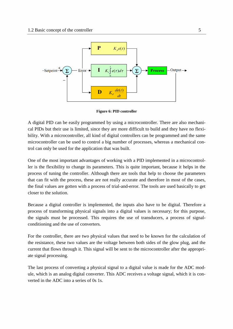
1.2 Basic concept of the controller 5
Figure 6: PID controller
A digital PID can be easily programmed by using a microcontroller. There are also mechani-
cal PIDs but their use is limited, since they are more difficult to build and they have no flexi-
bility. With a microcontroller, all kind of digital controllers can be programmed and the same
microcontroller can be used to control a big number of processes, whereas a mechanical con-
trol can only be used for the application that was built.
One of the most important advantages of working with a PID implemented in a microcontrol-
ler is the flexibility to change its parameters. This is quite important, because it helps in the
process of tuning the controller. Although there are tools that help to choose the parameters
that can fit with the process, these are not really accurate and therefore in most of the cases,
the final values are gotten with a process of trial-and-error. The tools are used basically to get
closer to the solution.
Because a digital controller is implemented, the inputs also have to be digital. Therefore a
process of transforming physical signals into a digital values is necessary; for this purpose,
the signals must be processed. This requires the use of transducers, a process of signal-
conditioning and the use of converters.
For the controller, there are two physical values that need to be known for the calculation of
the resistance, these two values are the voltage between both sides of the glow plug, and the
current that flows through it. This signal will be sent to the microcontroller after the appropri-
ate signal processing.
The last process of converting a physical signal to a digital value is made for the ADC mod-
ule, which is an analog digital converter. This ADC receives a voltage signal, which it is con-
verted in the ADC into a series of 0s 1s.

6 1 Introduction
One of the signals, which has to be read, is already a voltage signal whereas the other signal is
a current value. Because the ADC can only read a voltage signal, this current has to be con-
verted into a proportional voltage drop. For this purpose, there are different techniques that
will be explained later in this document.
Once the values, which are necessary, are in the form of a voltage signal, the next step is to
modify them, with the purpose of making sure that they are within the two limit values where
the ADC can read, as well as with the aim of getting the best precision. This process is called
signal conditioning.
Most of the time, in this process, the voltage is amplified and this can become a problem
when there is noise in the signal, since this noise will be also amplified. To avoid this from
happening, there are different techniques to be used, going from a correct layout of the com-
ponents to a filters design.
After these two processes, the signal can be inserted into the ADC. As it was said before, in-
side it there is a process that converts the input voltage into a digital output. This process de-
pends on the kind of ADC, and the election of it depends on each application. Later in this
document, the election of the ADC will be justified. Important aspects of this selection will be
the bits resolution and the frames per seconds.
After converting the signal, the microcontroller is ready to work with the digital values of
each signal and thanks to the program, that has been pre-configured in its memory program,
the appropriate control signal is given. This signal will switch on and off the circuit where the
glow plug is placed.
A mechanical switch cannot be used, since it will work at really high speed and this would
generate big amount of heat in the mechanical parts. Ruling out the mechanical switches, the
most common solution is the use of bipolar transistors, Mosfet, relays and optocoupler.
We use a switch because our glow plug will be always connected to a fixed voltage power
supply; in this way, with the switch, the power of the glow plug can be controlled.

7
2 MATLAB and Simulink
A Simulink model that simulates the behaviour of the engine was developed to know how the
different parameters, which have some kind of influence during the engine operation, change
and the influence that they have on glow plug temperature. Thanks to its graphical program-
ming environment, these different parameters can be directly displayed while the program is
running. For this reason, this program meant a quick and graphical tool to a better understand-
ing of how the engine works and what the desirable characteristic of the new controller will
be.
Furthermore, its communication with MATLAB allows to save the data after each simulation,
giving the possibility to compare different simulations to find out how the different condition
values affect engine performance.
With the purpose of saving this simulation to study further, a program in MATLAB was de-
veloped. This program permits to save data in a excel file after each simulation. It will be ful-
ly explained later in this document.
2.1 Brief description of the program
To explain the model, it can be split into three parts. The first part calculates the resistance
value variation that the glow plug suffers during its operation, the second part is related with
engine operation and its behaviour depends on which stroke the engine is and the third part is
the implementation of the PID controller.
The first part, previously defined as the one which calculates the resistance value, can be di-
vided at the same time into three processes: convective heat transfer, conductive heat transfer
and electric power for resistance heating. By constantly calculating the value of these three
processes, and using these results to calculate an energy balance, Simulink can obtain how the
resistance differs over the time. In this calculation the radiation heat transfer has been neglect-
ed, because its influence is low compare with the influence of the other processes.
In the second part, the simulation identifies in which of the four strokes the engine is working,
for each stroke a different subsystem is running. With this part, the conditions inside the com-
bustion chamber as well as the process of combustion are recalculated each time of the simu-
lation.
In the third part, a PID controller with omitted D value was implemented to control the tem-
perature of the glow plug. As the real controller, it reads the value of the current and voltage
that are placed in the glow plug, and from these values it calculates the current resistance val-
ue. After that, the current resistance value is compared with the set point value, getting the

8 2 MATLAB and Simulink
error and sending it to the PID. The PID controller according to its tuning parameters, gives
the new voltage value of the power supply. Figure 7 shows the set of blocks, which originally
was used for the control of the resistance value.
Figure 7: Blocks for PID controller of the original Simulink model
2.2 Development of the program
So as to adapt the model to the new proposal of controller, some changes were made, and lat-
er their influence in the overall engine performance was studied.
The first change was related to the reading resolution. Since the controller is digital, this al-
ways comes along with a digitization error. This error, due to the digital conversion, is an ap-
proximation to the original analogue value, the magnitude of it depends on the resolution of
the ADC.
To implement this in Simulink, a set of blocks of Gain, Rounding Function and Gain, were
used. They are illustrated in the Figure 8. The process is simple, and it just consists of multi-
plying the value by the resolution, rounding the result, and dividing it by the resolution. As it
can be seen, the upper set of block simulates the process of voltage reading and the bottom
block, the process of current reading.
The second variation is due to the process of power supply regulation. The new design of the
controller requires the power supply to be controlled by using a switch, this means that a
PWM signal to control this switch is required. The blocks that makes this transformation are
shown in Figure 9.

2.2 Development of the program 9
Figure 8: Blocks for selecting precision in the new Simulink model
In the figure below, inside the square the process of PWM signal creation is depicted.
MATLAB provides directly a block that can create a PWM signal by inserting the duty cycle
and configuring its frequency parameter. This block generates a PWM signal with an ampli-
tude of 1, thus a product block has to be added to give the signal the desirable amplitude, and
in this case, it is 11.
Although the original power supply has around 12V, in the simulation is used 11V since the
hot losses in the cables are not simulated in the model. In order a better simulation of what
really happens, a voltage drop in the cable of 1 V is assumed.
Figure 9: PWM signal transformation in the new Simulink model
As it can be seen, other changes have been made regarding to the original model, but they
were not done because of the use of the new controller, but because of the possibility of
Set blocks for PWM
generation

10 2 MATLAB and Simulink
changing these parameters when the MATLAB program is executed. This MATLAB program
will be explained in the following section.
2.3 Making tests with Simulink
For the process of testing with Simulink, a MATLAB program, which enables to run different
tests by only introducing the different constant values for each simulation, was developed. At
the same time, the data for each simulation will be stored in an excel file at the end of all the
simulations.
This program was programmed in two MATLAB files; the first one, where the different val-
ues are inserted by the user and the Simulink model is executed, and the second part where
the information for each simulation is stored in the excel file. How both parts work is ex-
plained in the following section.
2.3.1 Selecting values of the different parameters and running tests
In the beginning, a program, which asks for the value of the different parameters and runs the
Simulink model according to this configuration, was created. All this is done from the Com-
mand Window of MATLAB. Running the Simulink model can even be done from the com-
mand window, using the following structure:
The function is sim() and it is only required to write the name of the Simulink file between
two apostrophes.
MATLAB also allows using the variables of the workspace to execute a Simulink program,
by only writing the name of the variables inside the block configuration. This option gives a
good number of possibilities, for example a program that asks the user for the values of the
parameters, can be created. And later these parameters are used to run the Simulink model. To
do this, the next function is used:
The input() is the function, if something is written between the brackets using apostrophes,
this message will be shown in the Command Window. The value that is inserted by the key-
board is stored, in this example, in the variable “value”. This command is used in the program
inside a For loop to introduce the value of the different parameters.
2.3 Making tests with Simulink 11
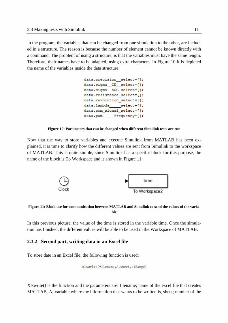
In the program, the variables that can be changed from one simulation to the other, are includ-
ed in a structure. The reason is because the number of element cannot be known directly with
a command. The problem of using a structure, is that the variables must have the same length.
Therefore, their names have to be adapted, using extra characters. In Figure 10 it is depicted
the name of the variables inside the data structure.
Figure 10: Parameters that can be changed when different Simulink tests are run
Now that the way to store variables and execute Simulink from MATLAB has been ex-
plained, it is time to clarify how the different values are sent from Simulink to the workspace
of MATLAB. This is quite simple, since Simulink has a specific block for this purpose, the
name of the block is To Workspace and is shown in Figure 11:
Figure 11: Block use for communication between MATLAB and Simulink to send the values of the varia-
ble
In this previous picture, the value of the time is stored in the variable time. Once the simula-
tion has finished, the different values will be able to be used in the Workspace of MATLAB.
2.3.2 Second part, writing data in an Excel file
To store date in an Excel file, the following function is used:
Xlswrite() is the function and the parameters are: filename; name of the excel file that creates
MATLAB, A; variable where the information that wants to be written is, sheet; number of the

12 2 MATLAB and Simulink
excel sheets where MATLAB will write and xlRange; which is the box where the data will be
written. The main problem of this code was to say MATLAB where it must write, because
Matlab cannot detect if one part of the excel sheet has already data. In Figure 12, it can be
seen how an Excel file looks likes after having written data in it.
Figure 12: Appearance of Excel data for saving data from Simulink tests
In the picture above, it can be seen that before each new test, Matlab writes the constants con-
figuration for the test, and then the different values for the variables for each moment of the
simulation.
2.4 Test trials
Simulink model was used with two main purposes. The first one was to know what kind of
influence the new conditions will have during engine working.
The second reason is because the glow plug is exposed to changing conditions, such as the
ones that happen during the combustion or during the entry of the mixture. With this simula-
tion, how they affect to its temperature can be known. Influence of new controller.
precision__select time CA50 P_HSI_averageP_HSI_var R_HSI R_HSI_var
16 50,00 2,4 25,05 0,006 0,8001 0,00015
sigma__CD__select 50,03 2,4 25,05 0,006 0,8001 0,00015
0 50,05 2,4 25,05 0,004 0,7998 0,00012
sigma__SOC_select 50,08 2,4 25,06 0,014 0,8001 0,00015
0 50,10 2,4 25,06 0,017 0,8000 0,00012
resistance_select 50,13 2,4 25,07 0,014 0,8001 0,00015
0,8 50,15 2,4 25,07 0,008 0,8001 0,00015
revolution_select 50,18 2,4 25,07 0,010 0,7995 0,00014
2000 50,20 2,4 25,06 0,009 0,8001 0,00015
lambda_____select 50,23 2,4 25,06 0,006 0,7999 0,00012
1,5 50,25 2,4 25,05 0,005 0,8001 0,00015
pwm_signal_select 50,28 2,4 25,05 0,006 0,8001 0,00014
0 50,30 2,4 25,05 0,006 0,8001 0,00015
pwm_____frequency 50,33 2,4 25,05 0,007 0,8001 0,00015
500 50,35 2,4 25,05 0,004 0,7998 0,00012
50,38 2,4 25,05 0,013 0,8001 0,00015
50,40 2,4 25,06 0,016 0,8000 0,00012
50,43 2,4 25,07 0,013 0,8001 0,00015

2.4 Test trials 13
2.4.1 Influence of new controller
Since the controller has to read the value of the current and the voltage digitally, an error
comes along with this process. As explained before, a set of blocks were used to simulate this
process and by changing their parameters, different values of precision were checked. The
influence of these values in the glow temperature is depicted in the Figure 13.
Figure 13: Influence in the resistance value due to the usage of different read resolution with Simulink
model (R_set= 0.80, sigmaSOC=0 , sigmaCD=0,rpm=1500, λ=1.5)
The Figure 13, shows how the behaviour of the resistance is, whose set point is 0.8Ω, for dif-
ferent values of resolution. The scale is 0.005 Ω/div, and the different signals are represented
with a different offset value for a better visualization.
As it can be seen in the figure, there is not a high influence of the resolution for the control of
the process, for a resolution of at least 12 bits. Only with resolutions of 8 and 10 bits, a varia-
tion from cycle to cycle can be appreciated.
The power supply for different resolution values also was checked and it is depicted in Figure
14.
0,798
0,799
0,800
0,801
0,802
0,803
45,0 45,5 46,0 46,5 47,0 47,5 48,0 48,5 49,0 49,5 50,0
Resis
tance [Ω
]
Time [s]
16 bits 14 bits 12 bits 10 bits 8 bits
0,005Ω/div
Offset (+0,003) (+0,002) (+0,001) (0) (-0,001)

14 2 MATLAB and Simulink
Figure 14: Influence in the power supply value due to usage of different read resolution with Simulink
model (R_set= 0.80, sigmaSOC=0 , sigmaCD=0,rpm=1500, λ=1.5)
In Figure 14 the power supply for the different precision are represented with a certain offset
value. The same results as in the other picture can be seen, for 12 14 and 16 bits the power
supply is almost the same, only using a resolution of 8 and10 bits a difference can be easily
appreciated.
Another modification that the use of the new control causes, is related with the way that the
control operates. The old controller modifies the value of the voltage of the power supply,
meanwhile the new one modifies the duty cycle of the signal that opens and closes the main
circuit. After implementing this new condition, two tests were made, using for both of them
the same parameters. The results for these two tests is depicted in Figure 15.
23,7
24,2
24,7
25,2
25,7
26,2
45 45,5 46 46,5 47 47,5 48 48,5 49 49,5 50
Po
we
r H
SI [W
]
Time [s]
16 bits 14 bits 12 bits 8 bits 10 bits
0,2 W/div
Offset (+0,9) (+0,6) (+0,3) (0) (-0,4)

2.4 Test trials 15
Figure 15: Comparison of Resistance control using the PWM and the voltage variable controllers with
Simulink (R_set= 0.80, sigmaSOC=0, sigmaCD=0, rpm=1500, λ=1.5)
As it can be seen, the influence of using PWM signal to regulate the power supply is bigger
than the influence of the resolution. According to the results, it can be said that the use of
PWM control adds a variation about 0.0003Ω to the resistance value. The frequency that was
used for this test has a value of 500 Hz.
2.4.2 Conditions in the combustion chamber
Since the engine is running at a speed of 2450 rpm, the condition in the combustion chamber
changes in a short period of time. This will have a big influence on the temperature of the
glow plug. Hence to be able to control it, what happened inside the combustion chamber must
be known.
As said before, the glow temperature is calculated from the heat of the convection and con-
duction process and the electric power of the glow plug. In Figure 16, the heat of both pro-
cesses is depicted. Because of the information explained before, the same power from these
two values has to be delivered by the power supply but with the opposite sign, in order to
keep the resistance value constant.
0,7990
0,7995
0,8000
0,8005
0,8010
0,8015
60 60,1 60,2 60,3 60,4 60,5 60,6 60,7 60,8 60,9 61
Resis
tance [Ω
]
Time [s]
Voltage Control PWM Control
0,005Ω/div
(Offset +0,001)

16 2 MATLAB and Simulink
Figure 16: Heat from the conduction and convection process affecting the glow plug during engine work-
ing with Simulink model (R_set= 0.75, sigmaSOC=0, sigmaCD=0,rpm=1500, λ=1.5)
As it can be seen in the figure above, the heat from conduction will be always negative, which
means the glow plug will always lose heat through this process. However the heat from con-
vection is both negative and positive, which makes sense owing to the engine cycle. The posi-
tive value of this process is because the combustion is happening and the hot surface is ex-
posed to hot residual gases, while for the rest of the time it has negative values.
Another important parameter that can be observed using the Simulink model is the tempera-
ture in the combustion chamber. As happened with the other two processes, the temperature
changes depending on which time of the cycle it is. This temperature is shown in Figure 17
along with the heat from convection. These two variables have a direct influence between
each other, since when the chamber temperature is bigger than the glow plug temperature, the
convection heat will be positive, and the same when it is lower, but the opposite.
-22,5
-22,4
-22,3
-22,2
-22,1
-22,0
-21,9
-60
-40
-20
0
20
40
60
80
24,6 24,65 24,7 24,75 24,8 24,85 24,9
Q c
onduction [W
]
Q c
onvection [W
]
Time [s]
Q convection
Q conduction

2.4 Test trials 17
Figure 17: Chamber Temperature and convective heat transfer (1 zone Woschni model) in the glow plug
with Simulink (R_set= 0.75, sigmaSOC=0 , sigmaCD=0,rpm=1500, λ=1.5)
0
400
800
1.200
1.600
2.000
-60
-40
-20
0
20
40
60
80
24,6 24,7 24,7 24,8 24,8 24,9 24,9
Q c
onvection [W
]
Cham
ber
Tem
petu
re [ºC
]
Time [s]
Q conduction
ChamberTemperature

18 2 MATLAB and Simulink

19
3 Circuit design and its components
With all information that was collected from the different tests with MATLAB, the necessities
for the controller were established. After that, the process of searching the right components
and the best solution for the controller started. To do this, the controller was divided into 4
parts, which are listed below:
A microcontroller.
Circuit to measure the voltage.
Circuit to measure the current.
Switch circuit.
This division is justified because the performance of each part can be checked regardless of
the others 3 parts.
In the next section, each part will be explained and justified. Also it is given information
about the chosen components as well as considerations related with the circuit layout.
3.1 Microcontroller
The most common solution for a controller is to use a digital controller, whose main part is
based on a microcontroller.
There is a large range of microcontrollers, so the selection of one of them is not an easy task,
the selection of Arduino microcontroller was based on its flexibility for operation. One of the
main characteristic is that it does not require an external circuit for its programming process.
It can be done directly by connecting Arduino board by USB with our computer.
As a brief introduction to microcontrollers, some of their most important characteristics as
well as its different parts will be clarified. These parts shared for almost all microcontrollers,
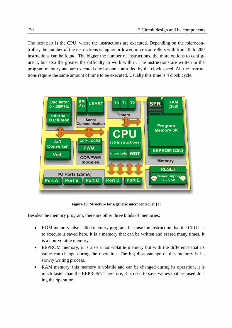
are shown in Figure 18.
In the top left part of the figure is the oscillator. The oscillator is the clock that controls the
operation of a microcontroller, this clock can be an internal signal or an external signal, de-
pending on the configuration. All the microcontrollers need a clock signal for the execution of
instructions with synchronism. By modifying the frequency of the oscillator, it can be
changed the working speed of the microcontroller as well as its power consumption and heat
generation, which are directly related with each other.
20 3 Circuit design and its components
The next part is the CPU, where the instructions are executed. Depending on the microcon-
troller, the number of the instructions is higher or lower, microcontrollers with from 35 to 200
instructions can be found. The bigger the number of instructions, the more options to config-
ure it, but also the greater the difficulty to work with it. The instructions are written in the
program memory and are executed one by one controlled by the clock speed. All the instruc-
tions require the same amount of time to be executed. Usually this time is 4 clock cycle.
Figure 18: Structure for a generic microcontroller [3]
Besides the memory program, there are other three kinds of memories:
ROM memory, also called memory program, because the instruction that the CPU has
to execute is saved here. It is a memory that can be written and erased many times. It
is a non-volatile memory.
EEPROM memory, it is also a non-volatile memory but with the difference that its
value can change during the operation. The big disadvantage of this memory is its
slowly writing process.
RAM memory, this memory is volatile and can be changed during its operation, it is
much faster than the EEPROM. Therefore, it is used to save values that are used dur-
ing the operation.

3.2 Circuit for voltage measurement 21
Usually the microcontrollers work with information coming from the outside or need to send
information to other processes. For the communication with the outside the microcontrollers
have serial communication modules. This microcontroller module is called I/O ports.
This information that is sent to the microcontroller does not often come in a digital form, but
in a voltage signal. For this reason, most of the microcontrollers have an ADC module that
enables to convert this signal into a digital one so that the CPU can work with it.
A way to exchange information with the outside has been explained, but it is not the only op-
tion, the microcontrollers also have communication modules that allow to exchange infor-
mation by using different protocols based on serial communication. Some of them have been
used in this project, and they will be explained later.
Another module is the timers module, which enables the microcontroller to calculates time or
events and according to this information executes operations. They are also used to generate
interactions. And of course a microcontroller needs a supply power, whose value is often 3.3
V or 5V and because the demanding of the current is very variable, it requires a bypass con-
denser close to this pin.
3.2 Circuit for voltage measurement
A conventional 12V automotive battery is used to feed the glow plug. Despite this, the volt-
age drop between both edges of the glow plug does not remain constant. The high value of the
current flowing through the circuit, creates a voltage drop in the cables that connect the glow
plug to the power supply, setting its voltage drop always lower than 12V.
Due to the continuous changes of the voltage drop in the glow plug, it is necessary to know its
instantaneous value in order to make an accurate calculation of its resistance.
Since a digital control will be implemented, to be able to work with this analog signal, firstly
it has to be transformed into a digital signal, using the ADC module. This ADC module,
which will be explained later, can convert a voltage value within a range of 0 to 5 V into a
digital value.
For this reason, the first requirement for this circuit is to convert the original value range of
the voltage drop into the range where the ADC can read. For doing this, there is a simple solu-
tion based on the use a voltage divider.
A voltage divider consists of a pair of resistors connected in series. The input voltage is ap-
plied across both the resistors and the output voltage emerged from the connection between

22 3 Circuit design and its components
them. This output is a fraction of the input voltage, which depends on the relation of the re-
sistance values of the two resistors.
In Figure 19 a scheme for a general voltage divider is depicted. The voltage value for the out-
put is calculated using the next formula:
𝑉𝑜𝑢𝑡 = 𝑉𝑖𝑛 ∙𝑅1
𝑅1 + 𝑅2
Figure 19: Scheme for a general voltage divider
This solution has a clear disadvantage, if a voltage divider is used, most of the values that are
in the range of the ADC will not be reached by the system. As a consequence, the sensitivity
will be much higher that if only the values that can be reached are included. The normal volt-
age drop values of the glow will be around 10-11.5 V, instead of the 0-12V. The Figure 20
shows the difference of sensitivity in both processes.
In order to get the biggest sensitivity, the purpose of the circuit is to transform the range of
10-11.5V into a new range of 0-5V. A solution is to use operational amplifiers along with a
voltage reference. The use of operational amplifiers gives a broad range of possibilities due to
the big number of configuration that can be built from them.
In order to do this, the first step is to compare the voltage between both edges of the glow
plug. With this purpose, the not inverted differential amplifier is used. Since the voltage drop
is bigger than the saturation limit of the amplifiers, the relation of the resistance values that
made up the configuration must be lower than 1, thus the output for this configuration will be

3.2 Circuit for voltage measurement 23
a fraction of the voltage drop in the glow plug. The scheme for this amplifier configuration is
shown in Figure 21.
Since the value of the resistor is 8.2 kΩ and 3.3 kΩ, the output of this circuit according to both
inputs will be:
𝑉𝑜𝑢𝑡 =3.3
8.2∙ (𝑉+ − 𝑉−)
In this way, for a voltage difference of 12V, the output will be 4.83 V, which is lower than the
saturation of the operational amplifier. This saturation is close to 5.5 V, as to a power supply
of ±7.5V is used.
Figure 20: Sensitivity comparison between the use a voltage divider and the use of the specific circuit for
voltage measurement

24 3 Circuit design and its components
In the next step, the output of this first amplifier is compared with the reference voltage, but
firstly this voltage has to be generated. In order to do this, a precision programmable refer-
ence along with resistor and a bipolar transistor are used. The use of the transistor is to make
the value of the voltage reference steady although small changes in the voltage level of the
power supply happen. Before the reference value is sent to the next differential amplifier a
buffer is used. A buffer is a kind of amplifier configuration where the output is the same as
the input and it is used to isolate the input circuit from the output circuit. The whole circuit
that is used to generate this voltage reference along with the buffer is shown in Figure 22.
Figure 21: non inverting differential amplifier use to compare the voltage between both edges of the glow
plug
As can be seen in the figure, also a potentiometer is used, this potentiometer allows to select
the voltage reference, and in this way the voltage from where the ADC will start to read can
be selected.

3.2 Circuit for voltage measurement 25
Figure 22: Circuit to generate a constant voltage reference
As it was explained before, now these two signals are compared, using also the non-inverting
differential configuration. Since in the output of this new amplifier either positive or negative
voltage values can appear, a rectifier has to be used in order to eliminate the negative values.
If a negative voltage value is send to the ADC, it might automatically be destroyed. Both am-
plifier configurations are depicted in Figure 23.
26 3 Circuit design and its components
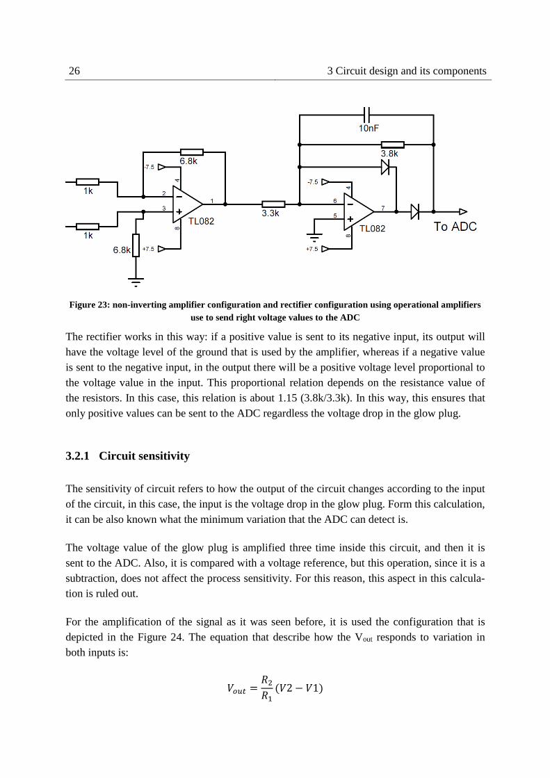
Figure 23: non-inverting amplifier configuration and rectifier configuration using operational amplifiers
use to send right voltage values to the ADC
The rectifier works in this way: if a positive value is sent to its negative input, its output will
have the voltage level of the ground that is used by the amplifier, whereas if a negative value
is sent to the negative input, in the output there will be a positive voltage level proportional to
the voltage value in the input. This proportional relation depends on the resistance value of
the resistors. In this case, this relation is about 1.15 (3.8k/3.3k). In this way, this ensures that
only positive values can be sent to the ADC regardless the voltage drop in the glow plug.
3.2.1 Circuit sensitivity
The sensitivity of circuit refers to how the output of the circuit changes according to the input
of the circuit, in this case, the input is the voltage drop in the glow plug. Form this calculation,
it can be also known what the minimum variation that the ADC can detect is.
The voltage value of the glow plug is amplified three time inside this circuit, and then it is
sent to the ADC. Also, it is compared with a voltage reference, but this operation, since it is a
subtraction, does not affect the process sensitivity. For this reason, this aspect in this calcula-
tion is ruled out.
For the amplification of the signal as it was seen before, it is used the configuration that is
depicted in the Figure 24. The equation that describe how the Vout responds to variation in
both inputs is:
𝑉𝑜𝑢𝑡 =𝑅2
𝑅1(𝑉2 − 𝑉1)
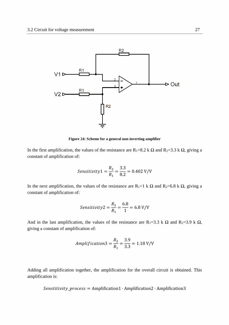
3.2 Circuit for voltage measurement 27
Figure 24: Scheme for a general non-inverting amplifier
In the first amplification, the values of the resistance are R1=8.2 k Ω and R2=3.3 k Ω, giving a
constant of amplification of:
𝑆𝑒𝑛𝑠𝑖𝑡𝑖𝑣𝑖𝑡𝑦1 =𝑅2
𝑅1=
3.3
8.2= 0.402 V/V
In the next amplification, the values of the resistance are R1=1 k Ω and R2=6.8 k Ω, giving a
constant of amplification of:
𝑆𝑒𝑛𝑠𝑖𝑡𝑖𝑣𝑖𝑡𝑦2 =𝑅2
𝑅1=
6.8
1= 6.8 V/V
And in the last amplification, the values of the resistance are R1=3.3 k Ω and R2=3.9 k Ω,
giving a constant of amplification of:
𝐴𝑚𝑝𝑙𝑖𝑓𝑖𝑐𝑎𝑡𝑖𝑜𝑛3 =𝑅2
𝑅1=
3.9
3.3= 1.18 V/V
Adding all amplification together, the amplification for the overall circuit is obtained. This
amplification is:
𝑆𝑒𝑛𝑠𝑡𝑖𝑡𝑖𝑣𝑖𝑡𝑦_𝑝𝑟𝑜𝑐𝑒𝑠𝑠 = Amplification1 ∙ Amplification2 ∙ Amplification3
28 3 Circuit design and its components
𝑆𝑒𝑛𝑠𝑖𝑡𝑖𝑣𝑖𝑡𝑦_𝑝𝑟𝑜𝑐𝑒𝑠𝑠 = 0.40 ∙ 6.80 ∙ 1.18 = 3.21 𝑉/𝑉
The meaning of this amplification is that if the voltage in the glow plug changes 1V, the volt-
age in the output of the circuit will change 3.21, therefore the sensitivity of the circuit is
3.21V/V.
Because the ADC can read values in a range of 5V and the sensitivity of our circuit is
3.21V/V, this means that it can be read a range of 1.56 V (5/3.21) regarding to the glow plug
voltage.
3.3 Circuit for current measurement
The other physic variable that has to be measured is the current. The ADC cannot directly
measure current, therefore firstly the current has to be converted into a proportional voltage
value. For doing this, there are different techniques, which were studied with the purpose of
finding the best one for the controller application. In the next section this different techniques
are explained.
3.3.1 Shunts
Use the famous Ohm’s Law to convert the current through a circuit in a drop voltage. The
Ohm’s Law says that I=V/R, so by placing a resistance with a known value, the value for the
current can be found out indirectly.
By reading this voltage value and then converting this value into current thanks to the relation
between voltage, intensity and resistance, the value of the resistance can be known.
Because a resistance is placed in the circuit, the working operation conditions suffer a slightly
modification, thus it will be advisable that the resistance value will be as low as possible. And
for this reason a shunt can only be placed in a circuit where galvanic isolation is not needed.
The advantage of this technique is that it can measure high current at high frequencies, and
using along with an operational amplifier, high precision can be reached taking into account
the ADC that is used.

3.3 Circuit for current measurement 29
3.3.2 Direct current current-transformer
These sensors work on the principle that when a magnetic core saturates, it loses its induct-
ance. A typical DCCT has an excitation winding wound onto a torroidal core which has
enough excitation to just drive it into saturation. A primary conductor is passed through the
core. The conductors current will modulate the core saturation which, in turn, will modulate
the second harmonic of the excitation current. This is then the monitored output. For mains
frequency applications, they can be excited using a sinusoidal main frequency voltage. Figure
shows DCCT principle.
Figure 25: Direct current transformer principle [4]
As the name suggests, DCCTs can measure DC and AC currents with galvanic isolation. The
strengths of these devices are simplicity and ruggedness against overload; if an appropriate
core material is selected, they are sensitive to low (<20mA) currents; their offset is stable over
a wide temperature range; and they offer good immunity to stray magnetic fields. But they
don’t have very good linearity; their frequency response is low (~500Hz) for a basic unit; they
have limited dynamic range of current; and the output may carry excitation noise. A single
core design injects noise into the primary circuit.
3.3.3 Open-loop Hall Effect current transducers
These fundamentally simple devices can, with the selection of appropriate components, ex-
hibit admirable performance. There are two distinct families: - units with a magnetic circuit
and units without. The latter technology simply uses a magnetic field strength sensor to meas-
ure the flux surrounding a current carrying conductor. Figure 26 shows a Hall Effect sensor
without magnetic circuit.
This is very simple and generally low cost technology and it is appropriate for some applica-
tions. Strong points are simplicity and low cost, providing galvanic isolation for measuring

30 3 Circuit design and its components
AC and DC currents; compact design especially when high (~150A) currents are to be meas-
ured; reasonable frequency response up to 50 kHz; and good signal to noise ratio for high
current sensing.
Weak points i.e. are very sensitive to stray
magnetic fields. Even the earth’s magnetic
field gives a 0.5A error. Stray fields could
arise from nearby conductors or contactor
coils. Needs to be located very close to the
current carrying conductor, this can then lead
to insulation and electrostatic screening issues.
Controlling the drift of offset voltage with
temperature can be quite a challenge. Gain
changes with temperature can be an issue.
The gain calibration of the devices will be
very loose, as their output is very dependent
on conductor position. This means that in-
process calibration probably will be required.
This technology may be worth a look if it is
necessary to measure reasonably high current
cheaply and can tolerate imprecision.
Because precision have a high importance in our measurement, this is not good solution for
the circuit.
3.3.4 Closed-loop hall effect current sensors
These sensors work on a principle similar to the open-loop Hall sensors, but include a feed-
back winding to null the flux in the core (Figure 7). GMR sensors may be used in place of the
Hall element. Because of the servo effect, excellent linearity results and gain become very
independent of temperature. The feedback coil and associated amplifier does add some cost
however.
The strong points i.e. are good DC and AC accuracy over a reasonable dynamic range. Low
insertion loss; good frequency response (~100 kHz); reasonable cost if a commitment made to
ASICs; good immunity to stray magnetic fields and electric fields with suitable screening.
Weaknesses, in turn, are dynamic range limited in practice by core hysteresis and null drift
with temperature; physically larger and costlier than open loop devices. Also, high quiescent
current particular when the primary current is high. This makes for self-heating which, in
Figure 26: Hall Effect without magnetic circuit [4]

3.3 Circuit for current measurement 31
turn, limits their use to lower ambient temperatures. These factors make them less attractive
for automotive applications.
The performance of closed-loop sensors has stabilized, while that of open loop continues to
progress with the introduction of new materials and components. There are now few instances
where closed-loop sensors are needed rather than their less costly open-loop counterparts.
3.3.5 Selection
Because its simplicity and its characteristics fit perfectly with the demands for the controller
circuit, the shunt resistor was chosen.
The shunt resistor that it is used in the circuit is shown in the Figure 27. Its main characteristic
is that it can deal with current up to 30 A offering a drop voltage of 75 mV and therefore its
resistance value is 2.5mΩ.
According to the normal resistance values of the glow plug during the working, the shunt will
generate around 0.3% of the heat that is generated in the glow plug.
Figure 27: HOBUT plate shunt SHR30A75 with a resistance of 0.00025Ω [RS online]
3.3.6 Scheme for the circuit
The idea for this circuit is similar to the idea of the circuit for voltage measurement. During
the normal engine working, there will be a current with a value around 10-14A, the goal for
this circuit is to convert this range of current into a voltage range of 0 to 5 V. As it was ex-
plained before, this is the range where the ADC can convert analog signals into digital sig-
nals.
32 3 Circuit design and its components
The first step to make this conversion requires to convert the current into a proportional volt-
age value. For this purpose, the shunt, which was selected before, is used. Due to its small
resistance value, the voltage drop in the shunt for this levels of current will be around 25 – 35
mV.
This voltage level is rather small to be read accurately by the ADC, thus an amplification of
this signal is required. For doing this an operational amplifier with a non-inverting differential
configuration is used. The scheme is shown in Figure 28.
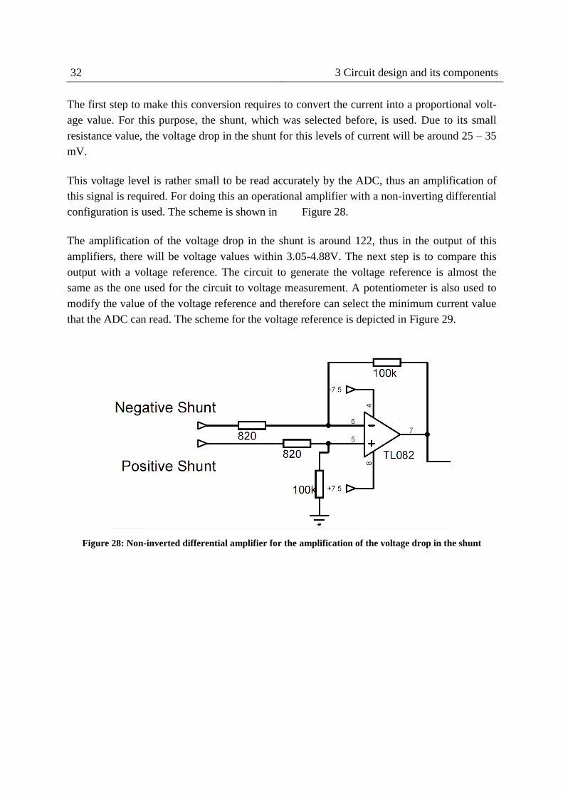
The amplification of the voltage drop in the shunt is around 122, thus in the output of this
amplifiers, there will be voltage values within 3.05-4.88V. The next step is to compare this
output with a voltage reference. The circuit to generate the voltage reference is almost the
same as the one used for the circuit to voltage measurement. A potentiometer is also used to
modify the value of the voltage reference and therefore can select the minimum current value
that the ADC can read. The scheme for the voltage reference is depicted in Figure 29.
Figure 28: Non-inverted differential amplifier for the amplification of the voltage drop in the shunt

3.3 Circuit for current measurement 33
Figure 29: Circuit that generate the voltage reference uses in the circuit for current measurement
Now, these two voltage are compared using also a non-inverting differential amplifier and the
output is sent to the precision rectifier. The scheme is shown in Figure 30.
Figure 30: Non-inverter differential amplifier and precision rectifier use in the circuit for voltage meas-
urement

34 3 Circuit design and its components
3.3.7 Circuit sensitivity
As it was done in the last circuit, the sensitivity of this circuit is also calculated. In this case,
its units are A/V, because it is measured how the voltage output changed compared with the
current of the circuit.
For this reason, in this process in addition to the different amplification stage, it has to be tak-
en into account the transformation that happened in the shunt.
The transformation that happened in the shunt is ruled by the value of its resistance, since it is
the variable that relates voltage and current. Since the output is current, the sensitivity of the
process is the resistance value of the shunt:
𝑆𝑒𝑛𝑠𝑖𝑡𝑖𝑣𝑖𝑡𝑦_𝑠ℎ𝑢𝑛𝑡 = 0.0025 𝑉/𝐴
For the amplification process, the same configuration as in the last circuit has been used, and
its scheme can be seen in Figure 24.
In the first amplification, the values of the resistance are R1=0.82kΩ and R2=100 kΩ, giving a
constant of amplification of:
𝑆𝑒𝑛𝑠𝑖𝑡𝑖𝑣𝑖𝑡𝑦1 =𝑅2
𝑅1=
100
0.82= 121.95 V/V
In the next amplification, the values of the resistance are R1=1 kΩ and R2=2.2 kΩ, giving a
constant of amplification of:
𝑆𝑒𝑛𝑠𝑖𝑡𝑖𝑣𝑖𝑡𝑦2 =𝑅2
𝑅1=
2.2
1= 2.20 V/V
And in the last amplification, the values of the resistance are R1=1 kΩ and R2=1.5 kΩ, giving
a constant of amplification of:
𝑆𝑒𝑛𝑠𝑖𝑡𝑖𝑣𝑖𝑡𝑦 3 =𝑅2
𝑅1=
1.5
1= 1.50 V/V
Putting the different amplification stages together, the amplification for the overall circuit is
obtained. This amplification is:
𝑺𝒆𝒏𝒔𝒕𝒊𝒕𝒊𝒗𝒊𝒕𝒚_𝒑𝒓𝒐𝒄𝒆𝒔𝒔 = 𝑺𝒆𝒏𝒔𝒊𝒕𝒊𝒗𝒊𝒕𝒚_𝒔𝒉𝒖𝒏𝒕 ∙ Sensitivity1 ∙ Sensitivity2 ∙ Sensitivity3

3.4 Digital Switch circuit 35
𝑆𝑒𝑛𝑠𝑖𝑡𝑖𝑣𝑖𝑡𝑦_𝑝𝑟𝑜𝑐𝑒𝑠𝑠 = 0.0025 ∙ 121.95 ∙ 2.2 ∙ 1.5 = 1.01 𝑉/𝐴
In this case, because the sensitivity of the process is 1.01V/A and the range of the ADC is 5V,
the range of current that the ADC will read will be 4.95A (5/1.01).
As it can be seen the values of the resistance have been selected, to reach this range, which
was the objective when the circuit started to be built
3.4 Digital Switch circuit
Since a power supply with a constant voltage is used, in order to regulate the power consump-
tion in the glow plug, the circuit is opened and closed successively.
For doing that, a switch between the glow plug and the power supply is placed. This switch is
controlled by a PWM signal that is sent by the microcontroller. A PWM signal is a signal with
two different voltage levels and a typical frequency. These levels are called on and off level
and the time that the signal remain in each level can be easily regulated by modifying their
duty cycle. The duty cycle describes the portion of time in “on” level regarding the signal
period and is expressed in percentages. An example of duty cycle is depicted in Figure 31.
Figure 31: Example of a PWM signal with its main characteristic
For the digital switch, there are several possibilities. Because the frequency that is required
for the application is more than 100 Hz, electromechanical switches were ruled out. The most
reasonable choice, due to the frequency of the application, is a solid state device.
For a solid state device, there are also different possibilities, such as a bipolar transistor,
Mosfet transistor and solid-state relay. Generally bipolar transistors are used for application
where the current levels are lower than 1A, so this option cannot be used for this application,
whereas a Mosfet, due to its low RDS(on), can work with high current values. A normal Mosfet

36 3 Circuit design and its components
can easily deal with current of 15 Amperes. Since the current for our application will be al-
ways lower than this value, this device was selected.
A Mosfet is a transistor that has three terminal; gate (G), source (S) and drain (D). It is con-
trolled by a voltage that is applied to the gate terminal. When the voltage, which is applied to
the gate, is bigger than a certain value, the device turns on and current can flow between
source and drain. This value of current is usually bigger than 8 V. In Figure 32, a scheme for
an N-channel Mosfet, as the use for the application, is depicted.
Figure 32: Scheme for an N-Chanel Mosfet
The problem for operating with the Mosfet is that Arduino PWM signal levels is 0 and 5V,
therefore, it is not enough for turning on the Mosfet. For this reason, a circuit that will amplify
the PWM signal is required. The objective of this circuit is to increase the voltage level of 5V
to at least a value that allows the transistor to be turned on and off.
For doing that a circuit that connects Arduino PWM signal with the gate terminal of the
Mosfet is used. This circuit is depicted in Figure 33.
In the circuit bipolar transistors are used. In this case, they are perfect for the application,
since the current flowing through them will be relatively low. The bipolar transistors are con-
trolled by current, and Arduino can provide enough current to control them. Furthermore, the
time for the switch on and off process is quite small. For all these reasons, they are the perfect
device to build up this circuit.
The circuit works in this way: the first transistor is connected to Arduino through its base ter-
minal, when Arduino is sending a high level, there will be current flowing from the base to
the emitter of the transistor and the transistor thus will be on. When there is a low level in
Arduino, the output of the transistor will be off.
3.4 Digital Switch circuit 37
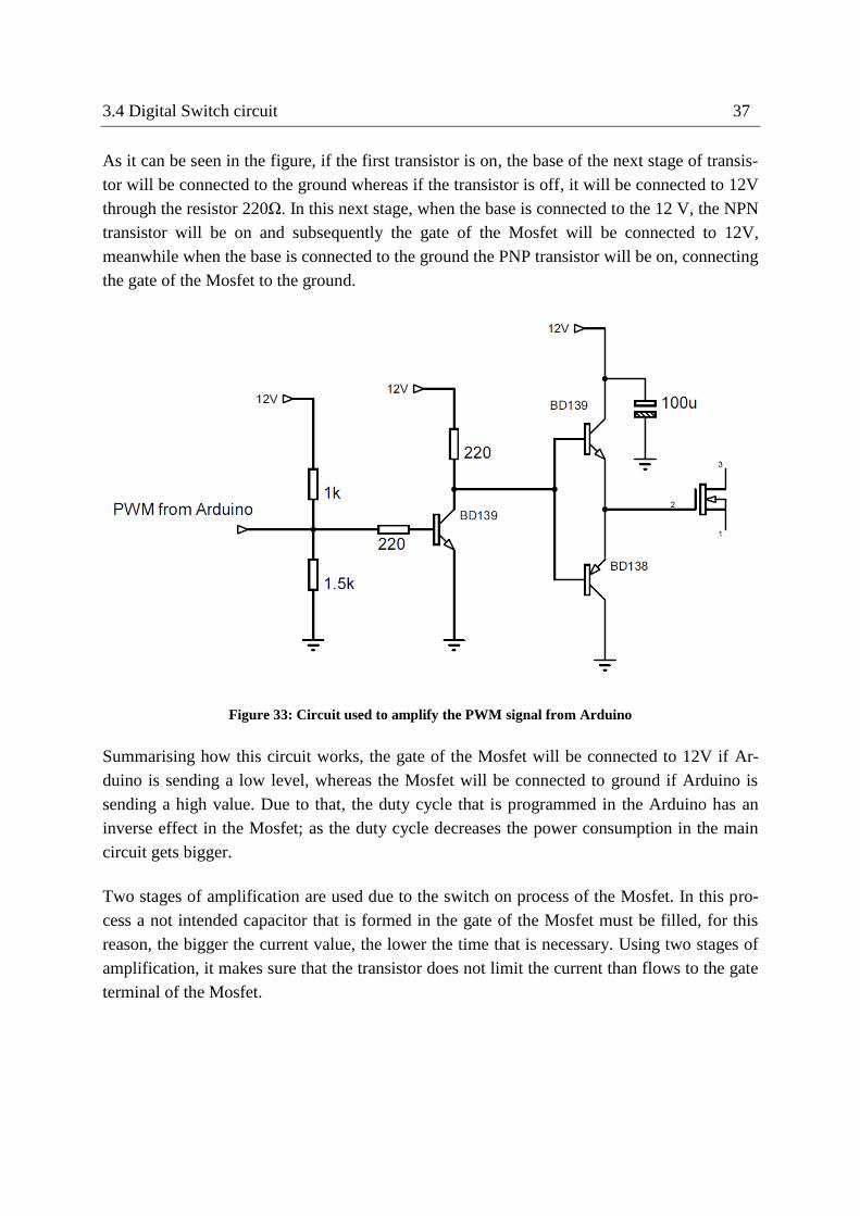
As it can be seen in the figure, if the first transistor is on, the base of the next stage of transis-
tor will be connected to the ground whereas if the transistor is off, it will be connected to 12V
through the resistor 220Ω. In this next stage, when the base is connected to the 12 V, the NPN
transistor will be on and subsequently the gate of the Mosfet will be connected to 12V,
meanwhile when the base is connected to the ground the PNP transistor will be on, connecting
the gate of the Mosfet to the ground.
Figure 33: Circuit used to amplify the PWM signal from Arduino
Summarising how this circuit works, the gate of the Mosfet will be connected to 12V if Ar-
duino is sending a low level, whereas the Mosfet will be connected to ground if Arduino is
sending a high value. Due to that, the duty cycle that is programmed in the Arduino has an
inverse effect in the Mosfet; as the duty cycle decreases the power consumption in the main
circuit gets bigger.
Two stages of amplification are used due to the switch on process of the Mosfet. In this pro-
cess a not intended capacitor that is formed in the gate of the Mosfet must be filled, for this
reason, the bigger the current value, the lower the time that is necessary. Using two stages of
amplification, it makes sure that the transistor does not limit the current than flows to the gate
terminal of the Mosfet.

38 3 Circuit design and its components

39
4 Components
4.1 Analog-to-digital converter (ADC)
Although, the microcontroller that is used in Arduino board has an internal ADC, an external
ADC was used. Since internal ADCs are placed so close to digital signals, these signals can
introduce additional noise. Therefore, the use of an internal ADC is not advisable, when a
good resolution is required for the application.
For this reason, the use of the internal ADC of Arduino was ruled out. Furthermore, the re-
sults using the engine model of Simulink, showed that working with a resolution of 10 bits,
has a small influence in the control process, and this influence almost disappeared when the
resolution was at least 12 bits. Bearing these two aspects in mind, an external ADC with at
least 12 bits resolution was desirable.
The ADC that was chosen for the controller was the MCP3208 manufactured by Microchip. It
is a Successive approximation ADC with 12 bits resolution. It has 8 input channels, which
allow the device to work either with a pseudo-differential or a single-ended input. The Figure
34 shows the pin configuration of the ADC.
Figure 34: ADC MCP3208 pin configuration [Datasheet]
The MCP3208 can operate over a broad voltage range (2.7 to 5.5 Voltage). When this voltage
is 5V, the maximum sample rate is 100 ksps whereas with a voltage of 2.7 is 50 ksps. For this
reason, it will be used 5 V as power supply.

40 4 Components
Regarding to the ADC architecture, a successive approximation (SAR) ADC use a circuit
called sample-and-hold (SHA) to save and keep the signal constant during the conversion
cycle. This voltage value is successively compared with the DAC using a comparator, which
determines whether the SHA output is bigger or not than the DAC output and sends the re-
sults to the successive-approximation register (SAR) as 0 to 1. This process is made as many
times as bits of resolution have the ADC, in a process of comparison to determine with the
minimum of operation the voltage of the sample taken. In Figure 35 a scheme of the architec-
ture of a successive approximation ADC is shown.
The process of conversion can be divided in two process, the first corresponds to the process
of storing the value in the SHA circuit. The component that is used for this purpose is fre-
quently a capacitor, thus enough time to store the value is required, and this time is called
Tsample. The second process is the comparison process, which requires one cycle of clock for
each bit of conversion. These two processes together give the conversion time that is usually
given in the components datasheet in unit of clock cycle. Thus the sampling rate will depend
on the frequency of the clock signal and on the times that are required to complete the reading
process.
Figure 35: Architecture for successive-approximation ADC [6]
Related with the communication of the ADC with the microcontroller or with other devices,
most of the SAR ADCs use a serial interface. In the case of the MCP3208, this communica-
tion is done using the Serial Peripheral Interface (SPI) bus.
The SPI bus is a synchronous serial communication interface used for short distance commu-
nication. SPI devices communicate in full duplex mode using a master-slave architecture with
a single master. The master device originates the frame for reading and writing.

4.1 Analog-to-digital converter (ADC) 41
It is a four-wire synchronous serial communication protocol. This four logic signal are:
- SCLK, it is the clock signal and is sent from the bus master to all slaves.4
- SS, it is the slave select signal, used to select the slave the master communicates
with;
- MOSI, it is the data line from the master to the slaves.
- MISO, it is the data line from the master.
A diagram for a SPI communication is depicted in Figure 36. In this case the master estab-
lishes communication with three devices. The communication can only be done between mas-
ter and slave, never between slaves. And the master can only communicate at the same time
with a slave.
Figure 36: Diagram for a SPI communication between a single master and multiple slaves [5]
The SPI communication between MCP3208 with the microcontroller, it requires to send
group of eight bits, also called byte. And the total number of bytes used to complete the
communication are three. The sequence of these 3 bytes is shown in Figure 37. As it can be
seen in the figure, the communication is initiated bringing the 𝐶𝑆 line low, the first and sec-
ond bytes of the Din line contain the Start information and the information related with the
selection of the kind of reading and the input where the value will be taken form. The second
and third bytes of the line Dout, contain the digital value of the sample voltage.

42 4 Components
Figure 37: SPI communication between MCP3208 ADC and Microcontroller
4.2 Liquid crystal display
A LCD is an electronic visual display that uses the light-modulating properties of liquid crys-
tals. They are prefect to display words or digits or even images with a low information con-
tent.
For the controller application, the LCD will be used to show the controller menu as well as
some data information such as resistance, voltage and current values. Since the glow plug will
be inside the engine, and it cannot been seen from the outside, the LCD give a quick and easy
way to visualize what it is happening in the glow plug during the engine working.
For the communication with the microcontroller, the LCD comes along with an I2C module.
This module allows the communication between the Arduino and the LCD display by using
the inter-integrate-circuit (I2C) bus. It is a serial, half duplex bus that uses two bidirectional
open-drain lines: Serial Data Line (SDA) and Serial Clock Line (SCL). The scheme for an
I2C communication is shown in Figure 39.

4.3 Push button 43
Figure 38: Scheme for a communication using I2C interface
The output is configured as an open collector; therefore, it has to be connected to Vcc using a
resistor, this combination is called pull up resistor. This configuration allows all the devices to
generate the same logic signal voltage level, enabling the communication between devices
with CMOs technology and TTL technology.
The communication is governed by a protocol. This communication always start with a
START condition that is received by all the slaves. Then the master sends the ADDRESS
along with the information of what kind of communication is wanted (Read or Written com-
munication).The address should fit one of the slaves addresses, starting the communication
with it after this generates a response called ACKNOWLEDGE signal. Now one of the device
send the data, depending on the kind of communication previously selected, and when it is
over, the master generates the STOP condition.
4.3 Push button
In order to scrolling through the program menu, push button are used. Each button is connect-
ed in one of its terminal to one analog input of Arduino. The other terminal is connected to
the 5V supply of Arduino. Also a pull down is used to make sure that the analogue input will
receive a 0V signal when the button is not pushed. In Figure 39, the connection is shown.

44 4 Components
Figure 39: Diagram for the connexion of the button with the respective analog input
In this way, when the button is pushed, the input will be high and during the rest of the time
the input will be low. With these buttons, it can be selected what data the display will show
and changed the set point of the glow plug.
4.4 Precision programmable reference
The device that was selected to generate the voltage reference was the TL431, manufactured
By Texas Instruments. It can generate a voltage reference from2.5 V to 36 V depending on
the external resistor. Its basic scheme is depicted in Figure 40.
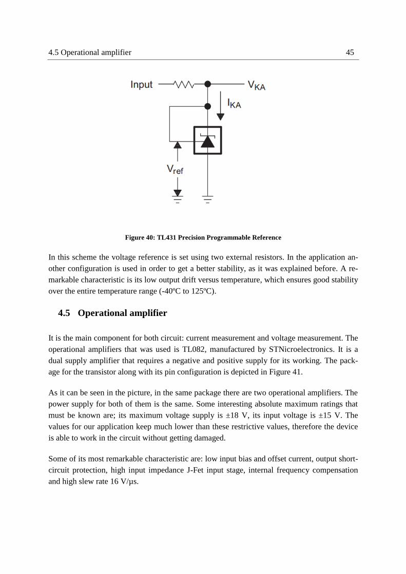
4.5 Operational amplifier 45
Figure 40: TL431 Precision Programmable Reference
In this scheme the voltage reference is set using two external resistors. In the application an-
other configuration is used in order to get a better stability, as it was explained before. A re-
markable characteristic is its low output drift versus temperature, which ensures good stability
over the entire temperature range (-40ºC to 125ºC).
4.5 Operational amplifier
It is the main component for both circuit: current measurement and voltage measurement. The
operational amplifiers that was used is TL082, manufactured by STNicroelectronics. It is a
dual supply amplifier that requires a negative and positive supply for its working. The pack-
age for the transistor along with its pin configuration is depicted in Figure 41.
As it can be seen in the picture, in the same package there are two operational amplifiers. The
power supply for both of them is the same. Some interesting absolute maximum ratings that
must be known are; its maximum voltage supply is ±18 V, its input voltage is ±15 V. The
values for our application keep much lower than these restrictive values, therefore the device
is able to work in the circuit without getting damaged.
Some of its most remarkable characteristic are: low input bias and offset current, output short-
circuit protection, high input impedance J-Fet input stage, internal frequency compensation
and high slew rate 16 V/µs.

46 4 Components
Figure 41: Package and pin configuration for the operational amplifier TL082 [Datasheet TL082]
Other different models of operation amplifier were tested, but it was the TL082, the one that
showed the best result. This result will be shown in the section of practical testing.
4.6 Noise considerations for the circuit design
The quality of the reading processes might depend mostly on the level of noise in the signal
that is sent to the ADC from the circuits for current and voltage measurement. For this reason,
the noise level has to be reduced to the minimum possible level, before being sent to ADC.
The first aspect to bear in mind, is the layout for the circuit.
In the datasheet of the ADC, some tips regarding the layout are given. When laying out circuit
board to be used with analog components, care should be taken to reduce noise wherever pos-
sible. Digital and analog traces should be separated as much as possible on the board, with no
traces running underneath the device or the bypass capacitor. Extra precaution should be tak-
en to keep traces with high frequency signals as far as possible from analog traces. In Figure
42, an example of a correct layout is shown.

4.6 Noise considerations for the circuit design 47
Figure 42: Example of a good layout in a board where there are digital and analog signal together [10]
Furthermore, the datasheet also recommends the use of an analog ground plane in order to
keep the ground potential the same for all the devices of the board.
The next step to reduce noise is to design analogue filters. An analog filter is a device that
removes from a signal some unwanted components or features. In this case, it wants eliminate
these signals whose frequency is not similar to the frequency of the system.
The filters that are used for this application are Low-pass filters. A low-pass filter passes sig-
nals with a frequency lower than a certain cut-off frequency and attenuates signals with fre-
quencies higher than the cut-off frequency. The amount of attenuation for each frequency
depends on the filter design. In this project, the values for the capacitor and the resistance
determine this cut-off frequency. In Figure 43, the Bode plot of a Low-pass filter is depicted,
whose cut-off frequency is 1000.
As it can be seen in the figure, the attenuation happens gradually from one specific value of
frequency. The cut-off frequency is defined as the value where the attenuation is -3 dB.

48 4 Components
Figure 43: Low-past filter with a cut-off frequency of 1000 Hz
In the design of a filter, the signal attenuation is not the only aspect that must be taken into
account. By placing filters, the response of the circuit is also modified, making its speed re-
sponse slower. For this reason, the filters design requires special attention.
During the filters design, the response was checked with the help of the oscilloscope for the
purpose of getting a trade-off between the speed response and the noise reduction.

49
5 Practical Testing
Before the construction of the final circuit, several tests and changes were made. No desirable
behaviour and dangerous situations for the different devices were corrected and avoided.
All electronic circuits are designed to work in specific working conditions. Nevertheless, not
desirable condition can happen. This anomalous behaviour can exceed some of the absolute
maximum rating values of the components and thus, they will be destroyed. To avoid this to
happen, circuit protections are used. The purpose of these circuits is not to change the normal
circuit working, they will work only under these anomalous situations.
When there are reading processes of a physical variable, a common problem is the noise that
can be placed in their analogue signal. This noise is caused either by components of the same
circuit or by external devices. To avoid this to happen, special attention in the design of the
circuit layout has to be paid. Furthermore, it can be reduced by using analog filters.
Owing to the use of electronic devices, another problem to be taken into account is their time
response delay. Furthermore, the use of filters increases the time circuit response. Since the
glow plug is working in a quick changed environment, the time response of the circuit has to
be relatively low. This response has to be kept much lower than the system frequency.
In the next section, it will be explained further different changes and tests that were made in
order to correct these working problems. Finally, it is described the improvement process of
circuit response.
5.1 Digital Switch circuit
As it was explained before, for this circuit a Mosfet along with a previous circuit transistor are
used.
Since this circuit only differences between high and low voltage values, the noise is not an
important problem. Nevertheless, because it has to turn on and off the main circuit, its time
response has a particular importance.
The time response for bipolar transistor is much faster than the Mosfet time response. There-
fore, it will be the time response of the Mosfet that determines mostly the overall time re-
sponse for this circuit.

50 5 Practical Testing
To know how a Mosfet responds, the datasheet provides information. This information is
generally given in 4 times that describe the Mosfet behaviour accurately. These four times
are:
Ton_delay; It is the time taken by the Mosfet to start turning on.
Toff_delay; It is the time taken by the Mosfet to start turning off.
Tfall; It is the time taken by the Mosfet to change from on to on.
Trise; It is the time taken by the Mosfet to change from off to off.
In Figure 44, these four time be visualized. In the picture it is represented the response of a
Mosfet when a voltage change in its gate terminal happens. The low level can completely turn
off the Mosfet, whereas the high level can turn it on.
Figure 44: Typical Time response for a Mosfet transistor
In addition to checking the parameters that the datasheet includes, the real response of the
transistor along with the circuit that connects it with the Arduino PWM output was checked.
For the tests, two different Mosfets were used and compared. In the next photos, the responses
0
5
10
Voltage [V
]
Time [s]
Gate Terminal Voltage
0
5
10
15
Curr
ent [A
]
Time [s]
Current Drain Source
Ton_delay
Tfall Trise
Toff_delay

5.1 Digital Switch circuit 51
of the Mosfets can be seen, and the time response can be analysed. The response when the
Mosfets are switching off can be seen in Figure 45 and Figure 46, while in Figure 47 and Fig-
ure 48 the response when they are switching on.
The Mosfets that were used were the IRFZ44N, manufactured by International Rectifier and
the TK42E12N1 manufactured by Toshiba. Both of them can deal with current bigger than
40A, therefore they can be perfectly used for the application.
Figure 45: IRFZ Mosfet switching off
Figure 46: Toshiba Mosfet switching on

52 5 Practical Testing
Figure 47: IRFZ Mosfet switching off
Figure 48: Toshiba Mosfet switching on
Analysing the results, the response of IRFZ Mosfet is faster than the one of Toshiba Mosfet in
the switch off process, whilst in the switch on process the response of Toshiba Mosfet is fast-
er.

5.1 Digital Switch circuit 53
Since there is not a big different between both Mosfets and the price of the Toshiba Mosfet is
much lower, the Toshiba Mosfet was selected.
Initially the circuit does not have the pair of resistances that work as a pull-up resistor. Due to
that, one Mosfet got damaged. When the Mosfet was connected to the power supply and glow
plug through its source and drain terminal, and Arduino was not sending any PWM signals,
there was current flowing through the main circuit. This unexpected behaviour happened be-
cause the voltage in the gate was bigger than the voltage in the source, and this made the
Mosfet to conduct. But because this voltage difference was not big enough, the Mosfet was in
the ohm region and therefore its resistance was much bigger than RDS(ON). As a result, a big
amount of heat was generated in Mosfet, ending up in its destruction.
In Figure 49 it is shown how the Mosfet regulates the current depending on its VDS. When the
Mosfet has a temperature of 25 C and the voltage Gate is 4.5 V, the current that can flow
through it is lower than 10 amperes, and this current becomes lower as the gate voltage de-
creases. For this reason, and because in the real application there will be a current bigger than
10A, this situation must be avoided.
Figure 49: Drain-to-Source Voltage versus Drain-to-Source Current for the Mosfet IRF44N [Datasheet]
To avoid that to happen, a pull-up resistor was set between the signal PWM, and the positive
terminal of the power supply. In this way, when there is no PWM signal, the Mosfet will be
closed.
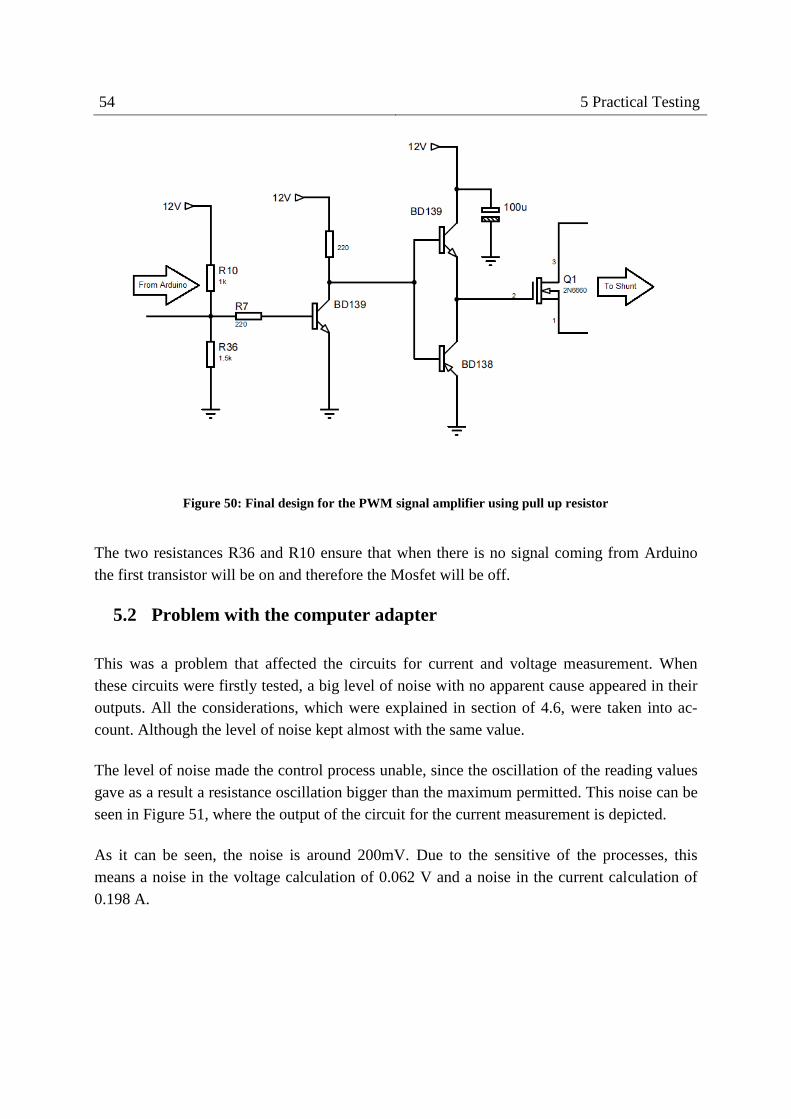
54 5 Practical Testing
Figure 50: Final design for the PWM signal amplifier using pull up resistor
The two resistances R36 and R10 ensure that when there is no signal coming from Arduino
the first transistor will be on and therefore the Mosfet will be off.
5.2 Problem with the computer adapter
This was a problem that affected the circuits for current and voltage measurement. When
these circuits were firstly tested, a big level of noise with no apparent cause appeared in their
outputs. All the considerations, which were explained in section of 4.6, were taken into ac-
count. Although the level of noise kept almost with the same value.
The level of noise made the control process unable, since the oscillation of the reading values
gave as a result a resistance oscillation bigger than the maximum permitted. This noise can be
seen in Figure 51, where the output of the circuit for the current measurement is depicted.
As it can be seen, the noise is around 200mV. Due to the sensitive of the processes, this
means a noise in the voltage calculation of 0.062 V and a noise in the current calculation of
0.198 A.

5.2 Problem with the computer adapter 55
Figure 51: Noise in the circuit of current measurement when computer adapter is working
In order to reduce the noise level, besides the techniques explained before, different kinds of
amplifiers were used, until the real cause of the problem was found.
In one of the countless tests, the real problem was discovered. In some way, the computer
adapter was generating this amount of noise in the signal. When the computer adapter was not
working, the noise was considerably reduced. In Figure 52 it is depicted the output signal of
the circuit measurement when the adapter is not used.
Figure 52: Noise in the output of circuit for current measurement when the computer adapter was not
working

56 5 Practical Testing
The noise level is around 50 mV when the adapter is not used. It must be noted, that all the
noise is not due to the circuit as voltage supply also has an internal noise. Anyhow, when the
adapter is not used the noise is reduced 4 times.
5.3 Circuits for current and voltage measurement
These two circuits are explained together since both of them shared the same problems and
thus the same solutions were applied. The components that are used for both circuits are the
same and their circuit schemes are highly similar.
The big problem, which was faced with these circuits, was related with the noise in their out-
puts. This problem was explained in the previous section, where it is clarified that it was a
problem due to the computer adapter.
Trying to solve this problem, different kinds of amplifiers were tested as well as their differ-
ent configurations. In this section the results for the different tests are shown, as well as it is
justified the final selection.
Depending in the power supply that is used, the operational amplifiers are divided into single-
supply and dual supply. The schemes for both configurations are shown in Figure 53.
Figure 53: Comparison between single supply op amp (Left) and dual supply op amp (right)
When op amps are powered from dual supplies, see figure above, the supplies are normally
equal in magnitude, opposing in polarity, and the centre tap of the supplies is connected to
ground.
Meanwhile when op amps are powered from single supply, its negative terminal is connected
to the ground of the circuit. It can be used one or another configuration for power supply, de-
pending on the amplifier to be used. There are op amps that can operate for both cases.

5.3 Circuits for current and voltage measurement 57
For the circuit, both configurations were tested, selecting one of them. The TL082 op amp for
working was used to work with dual supply whereas the LM 358 for single supply. This last
op amp can be used with both supply configurations but it is advisable to work with single
supply, since it was optimized for this working condition.
In the tests, the time response to a step input as well as the noise level were studied. In Figure
54 and Figure 55, the responses to a positive step input using both amplifiers are depicted.
Figure 54: Response to positive step input using TL082 amplifier
Figure 55: Response to positive step input using LM358 amplifier
In Figure 54, the response for the TL082 amplifier is represented, the time that it is necessary
to reach the final value is round 360µs. This time can be seen in a variable that appears in the

58 5 Practical Testing
picture with the name of BX-AX. While for the LM358 amplifier, the time that it is necessary
for the same step input is 4.120 ms, this means the LM358 is more than 10 times slower than
the TL082 responding to a positive step.
The same tests were made for a negative step input, and the results are represented in Figure
56 and Figure 57.
Figure 56: Response to negative step input using TL082 amplifier using the circuit for current measure-
ment
Figure 57: Response to negative step input using LM351 amplifier using the circuit for current measure-
ment

5.3 Circuits for current and voltage measurement 59
The time that is required for the TL082 to respond to a negative step is the same as the time
for the positive step, 360 µs. However, for the other amplifier this time is even higher, with a
value around 5.120 ms.
These two tests were made with the circuit for current measurement. Tests were also done
with the circuit for voltage measurement, and the results were similar. They showed a clear
advantage working with the TL082 amplifier. Although in this circuit it was more difficult to
identify the time response, since the power supply, as it is said in its manual, needs 3 ms to
respond to a change of voltage. The response of the power supply as well as the response for
the voltage circuit are depicted in Figure 58.
Figure 58: Response voltage measurement circuit
In the figure above, the power response is represented in blue, and it can be seen that it re-
quires a time to reach the final value. The voltage circuit response is represented in yellow. In
this case, it is not a response to a step input, so the response time cannot be identified.
After the results shown by the tests, it can be said that there is a clear advantage of the TL082
amplifier over the LM351 amplifier. For this reason, the first one was the selected amplifier
and the configuration that was used was the dual supply.
In order to get the dual supply used by the op amps, two resistor of the same value are placed
between the terminals of a power supply. In this way using this simple tension divider, the
ground reference for the op amps will appear between the resistors. Furthermore, the positive
terminal of the power supply will be used as a negative supply for the op amps and the same
with the negative terminal but the opposite.

60 5 Practical Testing
If the point between the resistors is connected directly to the different amplifiers, there will be
more current flowing through one resistor, therefore the ground will be not perfectly placed in
the middle voltage of the power supply. To avoid that to happen, a buffer amplifier is used.
Because the amplifier has a high input impedance, the current through the line taken from the
middle of both resistances will be so small that can be neglected.
The output for a buffer amplifier has the same value than its input. In this way, the ground as
well as the positive and negative supply for the op amps are gotten. The scheme for this small
circuit is shown in Figure 59.
Figure 59: Circuit with buffer amplifier to generate the ground reference for the amplifiers
5.4 Calibration of the circuits for current and voltage measurement
The circuits explained before sending voltage signals to the ADC. These signals are converted
into digital signals in the ADC and subsequently sent to the microcontroller. These digital
values represent voltage values but initially the relationship is unknown. In order to know this
relationship a calibration process is required.
Calibration is the process of finding the relationship between two quantities. In this case, be-
tween the digital value and its corresponding voltage or current value. To find this relation-
ship the current analogue value must be known. For this purpose a power supply, which ena-
bles to know the actual value of current and voltage, is used.
This power supply is used as a standard of the calibration. And by modifying the value of the
desirable variable it can be known the relationship between the two quantities for different
values and whether the relationship is linear or not.
For the voltage calibration, the power supply is connected directly to the circuit and it is not
necessary the current to be flowing whereas for the current calibration that is required. This

5.4 Calibration of the circuits for current and voltage measurement 61
makes the calibration of the current more difficult, since the values of the current to be cali-
brated are quite high to be kept for a long period of time. This makes the current calibration a
process much slower than the voltage calibration.
To know the value of the digital value, the monitor series of the Arduino IDE is used. This
monitor series is a window, where Arduino writes what was previously configured. In this
case, it is said that Arduino represents the digital value of voltage and current.
Once the simulation has finished, this data can be used to be compared with the corresponding
analog value. For this purpose, an excel file was used and the relationship was represented in
a graph. The current relationship is shown in Figure 60 and the voltage relationship is shown
in Figure 61.
Figure 60: Relationship between the analog value and digital value for the current using Arduino and the
external ADC to make the measurements
As it can be seen in both figures, the relationships, as it was expected, are linear for both cas-
es, so the relationship can be approximated with a first degree equation. This relationship is
inserted in the Arduino programme so that Arduino can transform automatically the digital
value into the appropriate value.
y = 0,0042x + 9,5781R² = 1
8
9
10
11
12
13
14
15
16
17
0 500 1000 1500 2000
Analo
g v
alu
e [
A]
Digital value

62 5 Practical Testing
Figure 61: Relationship between the analog value and digital value for the voltage using Arduino and the
external ADC to make the measurements
If a change in the circuit happens, for instance, the position of the potentiometer is modified,
the calibration of the circuit has to be done again.
y = 0,0042x + 9,5781R² = 1
8
9
10
11
12
13
14
15
16
17
0 500 1000 1500 2000
Analo
g v
alu
e [
A]
Digital value

63
6 Programming Arduino
The software that is used to write the program in the Arduino board is called Arduino IDE
(integrated development environment).This IDE is a cross-platform application written in the
programming language Java.
The Arduino IDE supports the languages C and C++ using special rules to organize code. The
Arduino IDE supplies a software library called Wiring from the Wiring project, which pro-
vides many common input and output procedures. A typical Arduino C/C++ sketch, shown in
Figure 62, consists of two functions that are compiled and linked with a program stub main()
into an executable cyclic executive program:
setup(): a function that runs once at the start of a program and that can initialize set-
tings.
loop(): a function called repeatedly until the board powers off.
Figure 62: Structure of Arduino IDE for a new project

64 6 Programming Arduino
Both functions setup() and loop() are required for the program to work. Setup() is used to ini-
tialize pin modes, start using libraries or begin serial communications. It must be included in a
program even if there are no statements to run. Loop() is the core of all Arduino programs and
does the bulk of the work.
Furthermore, at the beginning of the program, before the function setup(), part of the code is
written. In this part of code, it is included the necessary libraries and the global variables are
declared. Some special functions need to be initiated in this part as well.
One of the greatest advantages of working with Arduino is the different libraries that can be
found online. These libraries make the communication with external device easier, for in-
stance, in this project, a library for the communication with the display is used.
After this brief introduction to the Arduino program language, the code for the program will
be explained in the next section.
6.1 Programming code
To explain the code, it has been split into three part: beginning of the program, setup () and
loop ().
6.1.1 Beginning of the program
In this part it is not executed any code, it is used for including the variables and declaring the
global variables. Its function is to prepare the program so that the rest part of the code can be
executed.
The libraries that are used in this program are shown in Figure 63. These libraries are neces-
sary to establish connection with the ADC and the display and to run the controller.
Figure 63: Libraries used in the programing code of the controller
In relation with the use of the ADC and the display, a special initiate code must be pro-
grammed in this part of the program, for instance, the pins that will be used with this purpose
are declared.

6.1 Programming code 65
Finally, the different global variables are introduced. These variables are used in the whole
program, for this reason, they need to be declared in this part of the code. Variables that are
only used in a specific part will be declared in the specific loop.
6.1.2 Setup()
In the beginning of this part, the prescalers of the timer 0 and 3 are adjusted. These prescalers
determinate the frequency of the PWM signal. Each one is assigned to a specific pin, whose
PWM signal can be modified in terms of the frequency, for instance, the timer 0 is used for
pins 13 and 4.
This change is totally necessary, since the default frequencies for the pins are 490 Hz or 980
Hz and the designed system cannot work at these frequencies. The frequencies that are used
for the system are 60 Hz (in pin 4) and 120 Hz (in Pin 3). In Figure 64 it is shown the differ-
ent frequencies in pins 13 and 4 that are available by changing timer 0.
Figure 64: Different PWM frequencies for the different prescalers of the timer 0 in Pins 13 and 4
In this part of the code, the use of the libraries for the controller, the ADC and the display
requires some programming sentences. Furthermore, the serial communication of Arduino is
initiated.
Finally, due to the system working, the two digital outputs (pins 3 and 4) start sending the
PWM signal with a certain duty cycle. This is necessary, because the controller will become
unstable if it starts working with the glow plug at room temperature. To solve this problem,
during a period of time (around 10s) after the controller is initiated, current starts flowing
through the main circuit controlled by the PWM signal and thus the glow plug is heated up.
Meanwhile in the display can be seen a welcomed message. For its programming, the function
delay and a specific function for the LCD are used, this part of the code can be seen in Figure
65.

66 6 Programming Arduino
Figure 65: part of the code that generates the welcomed message and the time delay for the glow plug
heating
6.1.3 Loop()
This is the core part of the program, which will be executed until the microcontroller is shut
down or rebooted.
This part of the program can be split into two parts. The first part that includes the controller
operation as well as the data acquisition (digital values of current and voltage). The second
one, where the data to be shown in the display are programmed.
In the first part, the first thing to do is the acquisition of the digital values of current and volt-
age from the ADC. This process is programmed to be done only when there is current in the
main circuit. During the high level of the PWM signal, Arduino asks uninterruptedly the ADC
for the data, and during the low level, the mean value is calculated using these data, getting
the digital value of current and voltage for the cycle.
After this, and thanks to the relationship, these digital values are converted into the appropri-
ate analog values. Then the resistance and subsequently the error are calculated. Afterwards
the code of the controller uses this error to modify the duty cycle of the signal.
The second part is programmed with different IF loops. The program will enter to one of them
depending on the selection of the user through the bottom
This part is only executed each time that the first part is executed a certain number or times
(in the code this number is 40 but it can be modified). The reason is because of the visualiza-
tion of the information in the display; otherwise, the data will be constantly changing making
it impossible to read the values.

67
7 Fast Adaptive Saturated (FAS) Controller
The name of the controller come from the way it operates. It has two principal characteristic;
its three ranges of operation, which are explained later, and the saturation, because the change
in the duty cycle is concentrated in the first cycles after the error happens and then it remains
the same value.
In the beginning, A PID controller was programmed in the Arduino board in order to control
the temperature of the glow plug. However, the results showed using a PID, were not as good
as expected. These tests show in this section were all done with the glow plug working out-
side the engine.
For this reason the response of the system to different changes of the duty cycle was studied.
Thanks to these tests, it could be appreciated more accurately how the glow plug works and
gave an idea of what the controller should make.
The tests shown in this section were all done with the glow plug working outside the engine.
When the glow plug was tested inside the engine, a problem came up. This problem will be
explained in the next section.
7.1 Controller operation
The controller operation is divided into three range, whose behaviours are totally different.
Each region has its own justification that will be explained later. Firstly, they are introduced:
Range 1: |error|<0.5 mΩ. Value of the new duty cycle:
Error positive (Previous)Duty cycle)+4 Previous Duty cycle
Error negative Previous Duty cycle (Previous Duty cycle)+4
Range 2: 0.5 mΩ<|error|>4 mΩ. Value of the new duty cycle:
Previous Duty cycle – (error · constant)
Range 3: |error|>4mΩ. Value of the new duty cycle:
Error positive (Previous Duty cycle) + Limit variation per cycle
Error negative (Previous Duty cycle) – Limit variation per cycle

68 7 Fast Adaptive Saturated (FAS) Controller
The first range works when the error is quite small. It was programmed with the objective of
reducing the error when the temperature in the glow plug is steady. The reason for this is that
the reading process has a variation of around 0.5 mΩ; therefore, when stability is reached, for
the actual glow plug temperature, different values can be measured, being these values in a
range of 0.5 mΩ. Using a PID creates an oscillation bigger than 2 mΩ, so a different behav-
iour for this range was programed.
This range works as a controller of two state. When the error is positive, it gives a certain duty
cycle, when the error is negative, it makes this duty cycle increase by 4 the objective of this
duty cycle is that the measurement of the temperature moves from positive to negative or
negative to positive each cycle, remaining always inside this range.
With this range, the stationary error of the controller is lower than 0.5 mΩ.
The second range woks when the value of the error is moderately big. The duty cycle is gov-
erned by a constant value. In this range, the controller works like a PID with only integral
part. Each cycle, a modification of the duty cycle is calculated using the formula shown be-
fore. In this way, the duty cycle can be changed each cycle when the error is in this range.
The third part works when the error is quite big. There is a maximum variation of the duty
cycle, and in this range this maximum variation is reached. Therefore, when the error is in this
range, this maximum variation will be added to the previous duty cycle value each cycle. This
maximum variation will be positive or negative depending on whether the error is negative or
positive.
For a better understanding of how this three ranges work, a graph is shown in Figure 66.

7.2 Test of the controller working 69
Figure 66: The variation of the duty cycle depending on the error for the three range of the controller
Besides these three ranges, there is another fact that enables this controller to respond faster
and without oscillation. For the variation of the duty cycle a limit was established, where the
controller enters in a saturation state. The controller can only increase or reduce its value by
30 during 0.5s. With this limit, once a big error happens, there is only variation in the duty
cycle during the first cycles after the error is detected. Once this limit duty cycle time varia-
tion is reached, its value remains the same until the sign of the error changes or after 0.5 s.
7.2 Test of the controller working
With the three ranges for the controller previously defined, the search for the best parameters
started. Firstly the response to a modification in the set point was studied.
The set point was increased and decreased, studying the time and the shape of the response to
this variation. With the different responds, it was tried to identify what possible variations in
the parameters can make the response better. One of these initial tests is shown in Figure 67.
Range 1
Range 2
Range 3

70 7 Fast Adaptive Saturated (FAS) Controller
Figure 67: Initial test of the glow plug temperature working with the FAS controller
As it can be seen in the picture, the set point was increased and decreased by 0.02 and an
anomalous behaviour in this test happens. When the set point is decreased, an oscillation dur-
ing the first cycles after the set point is reached happens. The cause of this behaviour was due
to a low value of the duty cycle. Due to this low duty cycle, the main circuit was active only
during a quite short period of time, making the ADC unable to read enough values and thus
the resistance calculation varied too much. For this reason a limit for the duty cycle was es-
tablished. Figure 68 shows the final results once this problem was solved.
In Figure 68, it can be seen how these oscillations have been completely eliminated, and even
for lower values of resistance, these oscillations do not appear. Regarding to the new re-
sponse, it can be seen that the controller responsds even faster. However for low glow plug
temperature, when a positive change in the set point happens, the response of the controller
has a not desirable overshoot. This problem could not be solved without making the response
slower. For this reason, this behaviour was considered to be good.
0,75
0,77
0,79
0,81
0,83
0,85
0,87
0,89
0 5 10 15 20 25 30 35 40 45
Resis
tance [Ω
]
Time [s]

7.2 Test of the controller working 71
Figure 68: Final test of the glow plug temperature working with the FAS controller
Furthermore, the stationary response was also studied. Initially when the controller started to
be designed, the first range of the controller was not used. It was after its stationary response
was analysed, when this range was added. It was obvious that a special behaviour was neces-
sary when the error was smaller than a certain error.
Figure 69: Stationary error of the glow plug temperature working with the FAS controller in its first stage
of development
0,69
0,71
0,73
0,75
0,77
0,79
0,81
0,83
0,85
0 10 20 30 40 50 60 70 80 90
Resis
tance [Ω
]
Time [s]
0,8195
0,82
0,8205
0,821
0,8215
10 11 12 13 14 15 16 17 18 19 20
Re
sis
tan
ce
[Ω
]
Time [s]
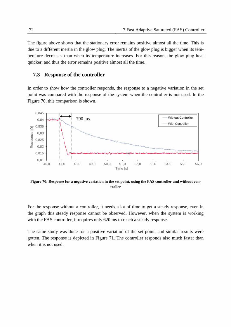
72 7 Fast Adaptive Saturated (FAS) Controller
The figure above shows that the stationary error remains positive almost all the time. This is
due to a different inertia in the glow plug. The inertia of the glow plug is bigger when its tem-
perature decreases than when its temperature increases. For this reason, the glow plug heat
quicker, and thus the error remains positive almost all the time.
7.3 Response of the controller
In order to show how the controller responds, the response to a negative variation in the set
point was compared with the response of the system when the controller is not used. In the
Figure 70, this comparison is shown.
Figure 70: Response for a negative variation in the set point, using the FAS controller and without con-
troller
For the response without a controller, it needs a lot of time to get a steady response, even in
the graph this steady response cannot be observed. However, when the system is working
with the FAS controller, it requires only 620 ms to reach a steady response.
The same study was done for a positive variation of the set point, and similar results were
gotten. The response is depicted in Figure 71. The controller responds also much faster than
when it is not used.
0,81
0,815
0,82
0,825
0,83
0,835
0,84
0,845
46,0 47,0 48,0 49,0 50,0 51,0 52,0 53,0 54,0 55,0 56,0
Re
sis
tan
ce
[Ω
]
Time [s]
Without Controller
With Controller
790 ms
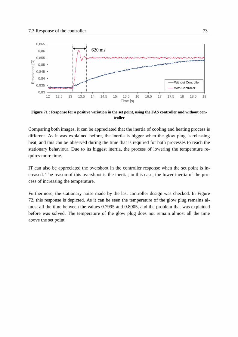
7.3 Response of the controller 73
Figure 71 : Response for a positive variation in the set point, using the FAS controller and without con-
troller
Comparing both images, it can be appreciated that the inertia of cooling and heating process is
different. As it was explained before, the inertia is bigger when the glow plug is releasing
heat, and this can be observed during the time that is required for both processes to reach the
stationary behaviour. Due to its biggest inertia, the process of lowering the temperature re-
quires more time.
IT can also be appreciated the overshoot in the controller response when the set point is in-
creased. The reason of this overshoot is the inertia; in this case, the lower inertia of the pro-
cess of increasing the temperature.
Furthermore, the stationary noise made by the last controller design was checked. In Figure
72, this response is depicted. As it can be seen the temperature of the glow plug remains al-
most all the time between the values 0.7995 and 0.8005, and the problem that was explained
before was solved. The temperature of the glow plug does not remain almost all the time
above the set point.
0,83
0,835
0,84
0,845
0,85
0,855
0,86
0,865
12 12,5 13 13,5 14 14,5 15 15,5 16 16,5 17 17,5 18 18,5 19
Re
sis
tan
ce
[Ω
]
Time [s]
Without Controller
With Controller
620 ms

74 7 Fast Adaptive Saturated (FAS) Controller
Figure 72: Stationary error of the glow plug temperature working with the FAS controller in its last stage
of development
0,7985
0,7990
0,7995
0,8000
0,8005
0,8010
0,8015
10 20 30 40 50 60 70
Re
sis
tan
ce
[Ω
]
Time [s]
0,7990
0,7995
0,8000
0,8005
0,8010
31 32 32 33 33
Re
sis
tan
ce
[Ω
]
Time [s]

75
8 Problem working with the engine
As it was mentioned before, a problem happen with the controller circuit when the glow plug
works inside the engine. This problem is due to the installation ground, which it is connected
to one edge of the glow plug.
Due to safety reasons, the engine has to be connected to the installation ground. Since the
engine is connected to one part of the glow plug, this part is also connected to the ground.
Therefore this part of the glow part remains in a constant level of voltage, since the ground of
the installation has a big inertia.
Because this part of the glow plug remains in constant voltage level, the ground that is used
for the controller circuit is constantly changing. This change in the ground inserts noise in the
measurement process of the voltage and the current, making the controller unable to keep the
value of the resistance steady.
Figure 73: Switch circuit scheme to show the two different grounds
As it can be seen in the figure, in the circuit, the negative terminal of the battery is connected
to the ground of the controller circuit. When the Mosfet opens the circuit, the ground of the
circuit has a voltage of -12 V respect to the installation ground, since the ground of the instal-
lation is connected to the positive terminal of the battery. While when the Mosfet closes the
circuit, the ground of the installation is connected to the negative terminal and due to the cur-
rent, the ground of the circuit have a voltage lower than the ground of the installation. This
value depends on the losses in the cables, transistor and shunt and is around 1 to 2 V.

76 8 Problem working with the engine
For this problem, there is a solution. This solution is based on the insulation of both circuits;
in this way, the ground of the controller circuit has not to be connected to the negative termi-
nal of the battery. To do this, an optocoupler is used in the switch circuit. Instead of the first
bipolar transistor, an optocoupler is placed. The design of this circuit can be seen in Figure
74.
Figure 74: Switch circuit with optocoupler to solve the problem of the installation ground
Although the circuit could not work inside the engine, the controller was checked during the
engine working. The FAS controller was programmed in the computer that was the responsi-
ble to control a power supply by modifying its voltage value. And later, the engine was oper-
ated using the glow plug controlled by the FAS controller.
The results showed that the new controller allowed for a significant improvement of control-
ler performance. The resistance value kept almost steady and it allowed to modify the set
point for the glow plug during the engine working without becoming unstable. In spite of the
good performance of the new controller, the cycle-to–cycle variations remained high, being
much bigger than the normal values during spark ignition operation.
77
9 Conclusion
The circuit that was built to control the glow plug was able to remain the stationary error val-
ue around 0.0005Ω and showed good response to changes in external conditions. With regard
to the components that made up this circuit, the shunt resistor responded with high speed to
the different changes and with an almost perfect linearity; hence it can be said that it is a right
technique fort these applications. Moreover, the use of operational amplifiers along with the
voltage reference allowed selecting the ranges of both measurements that wanted to be read.
The negative aspect of the performance of this circuit is the noise in the measurements. This
noise depends mostly on the noise of the signals that are sent to the ADC, so the use of an
ADC with more resolution will not improve its performance. In order to reduce this noise, it is
necessary to narrow the range of temperature where the glow plug can operate, so that it al-
lows further amplification of both signals, and, as a consequence, the influence of the noise
over the measurements will be reduced.
Furthermore, due to the connexion of one edge of the glow plug to the ground of the installa-
tion, it requires the isolation between the battery and the power supplies that are used to feed
the microcontroller and the circuit.
Concerning the performance of the controller, the use of the FAS controller has shown that it
is possible to maintain the resistance value of the glow plug highly stable during engine oper-
ation. However, cycle-by-cycle variations in the start of combustion remain high, which leads
to the conclusion that combustion stability would not profit from further optimisation of this
type of constant-temperature controller.
Since the temperature remains steady in the surface of the ignition system, the start of the
combustion is highly reliant on the local conditions that happen close to the glow plug. As a
consequence, the start of the combustion fluctuates.
In order to reduce the cycle-by-cycle variation, a new behaviour of the controller is proposed.
Instead of keeping the temperature steady, the controller must work with two levels of tem-
perature. One of those levels corresponds to the temperature of the glow plug when combus-
tion starts, whereas the other level of temperature must be reached for the glow plug during
the rest of the time. The difference between those two levels will depend on the inertia of the
system, that is, how fast the temperature of the glow plug can be decreased or increased.
With this controller, the start of combustion becomes also dependent of the glow plug tem-
perature, making lower the influence of the internal conditions. And in this way, the cycle-to-
cycle variation might decrease.

78 Conclusion
To conclude, this study has shown a method of implementing a controller with better stability
and faster response. However, this was a proposal which leaves the door open to further re-
search.

79
Bibliography
[1] Denis Neher, Fino Scholl, Victor Teschendorff , Maurice Kettner “Controlled Hot
Surface Ignition in Stationary Petrol and Natural Gas Operation” August 2012.
[2]
Fino Scholl, Dnis Neher, Maurice Kettner, Andrés Melgar Bachiller, Markus Klaissle
“ Effects of Intake Pressure and Air-Fuel Ratio on Controlled Hot Surface Ignition
operating with Natural Gas” August 2015.
[3] F. School, D.Neher, M.Kettner, M.Klasisle, A.Melgar “Effects of Intake Pressure and
Air-Fuel Ratio on Controlled Hot Surface Ignition Operating With Natural Gas” No-
vember 2015.
[4] D. Neher, F. Scholl, V. Teschendorff, M.Kettner “Controlled Hot Surgace Ignition in
Stationary Petrol and Natural Gas Operation” 2012-32-0006/JSAE 201290006.
[5] Milan Verde “PIC Micorontrollers Programing in Basic” 2010 by MikroElektronic
[6] Warren Pettigrew, CTO Raztec Sensors “Selecting the Most Effective Current Sensing
Technology”
[7] Sergio Noriega “Apuntes de Clases; Circuitos Generadores de Reloj” Universidad
Nacional de la Plata 20003
[8] Wikipedia online encyclopaedia “Serial Peripheral Interface Bus”
[9] Walt kester “Which ADC Architecture is Right for Your Application”
[10] Bonnie C. Baker Microchip Technology Inc. “Layout Tips on 12-Bits A/D Converter
Application”
[11] Texas Instruments “Choose the right A/D converter for your application”
[12] Texas Instruments “Current Shunt Monitors” 2014
[13] Jinghua Zhong “PID Controller Tuning: A Short Tutorial” Spring,2006.
[14] Omege “Temperature Control; Tuning a PID (Three Mode) Controller.
[15] Klemens Gintner “FTB731 Sensorik/Sensors” Winter Semester 2015-2016.
[16] Universisdad de El Salvador, Escuela de Ingeniería Eléctrica “Capitulo I-
Amplificadores Operacionales.
[17] Analog Devices “Operational Amplifiers Selection Guide” 20111-2012
[18] Texas Instruments “Active Filter Design Techniques”
[19] Vrej Brakhordarian, International Rectifier “Power Mosfet Basics”
[20] Fairchild Semiconductor “Bipolar Power Transistor Selection Guide”
[21] Bruce Carter and Thomas R.Brown, Texas Instruments “Handbook of operational am-
plifier application” SBOA092A-October 2001.
[22] Perry Miller and Doug Moore, Texas Instruments “Precision voltage references”

80 Bibliography

81
Table of Figures
Figure 1: Correlation Resistance-Temperature for the glow plug [1] ................................................................ 1
Figure 2: Previous close-loop temperature control of the hot surface ignition system [1] ................................ 2
Figure 3: Combustion centre CA50 over HSI resistance for relative air-fuel ratios 1.74-1.84 [2] ....................... 2
Figure 4: Diagram for a generic open-loop control ........................................................................................... 4
Figure 5: Diagram for a generic close-loop control ........................................................................................... 4
Figure 6: PID controller .................................................................................................................................... 5
Figure 7: Blocks for PID controller of the original Simulink model .................................................................... 8
Figure 8: Blocks for selecting precision in the new Simulink model .................................................................. 9
Figure 9: PWM signal transformation in the new Simulink model .................................................................... 9
Figure 10: Parameters that can be changed when different Simulink tests are run ........................................ 11
Figure 11: Block use for communication between MATLAB and Simulink to send the values of the variable . 11
Figure 12: Appearance of Excel data for saving data from Simulink tests ....................................................... 12
Figure 13: Influence in the resistance value due to the usage of different read resolution with Simulink model
(R_set= 0.80, sigmaSOC=0 , sigmaCD=0,rpm=1500, λ=1.5) .................................................................... 13
Figure 14: Influence in the power supply value due to usage of different read resolution with Simulink model
(R_set= 0.80, sigmaSOC=0 , sigmaCD=0,rpm=1500, λ=1.5) .................................................................... 14
Figure 15: Comparison of Resistance control using the PWM and the voltage variable controllers with
Simulink (R_set= 0.80, sigmaSOC=0, sigmaCD=0, rpm=1500, λ=1.5) ...................................................... 15
Figure 16: Heat from the conduction and convection process affecting the glow plug during engine working
with Simulink model (R_set= 0.75, sigmaSOC=0, sigmaCD=0,rpm=1500, λ=1.5) .................................... 16
Figure 17: Chamber Temperature and convective heat transfer (1 zone Woschni model) in the glow plug with
Simulink (R_set= 0.75, sigmaSOC=0 , sigmaCD=0,rpm=1500, λ=1.5) ...................................................... 17
Figure 18: Structure for a generic microcontroller [3] ..................................................................................... 20
Figure 19: Scheme for a general voltage divider ............................................................................................. 22
Figure 20: Sensitivity comparison between the use a voltage divider and the use of the specific circuit for
voltage measurement ........................................................................................................................... 23
Figure 21: non inverting differential amplifier use to compare the voltage between both edges of the glow
plug ....................................................................................................................................................... 24
Figure 22: Circuit to generate a constant voltage reference ........................................................................... 25
Figure 23: non-inverting amplifier configuration and rectifier configuration using operational amplifiers use
to send right voltage values to the ADC ................................................................................................ 26
Figure 24: Scheme for a general non-inverting amplifier ................................................................................ 27
Figure 25: Direct current transformer principle [4] ......................................................................................... 29
Figure 26: Hall Effect without magnetic circuit [4] .......................................................................................... 30
Figure 27: HOBUT plate shunt SHR30A75 with a resistance of 0.00025Ω [RS online] ...................................... 31
Figure 28: Non-inverted differential amplifier for the amplification of the voltage drop in the shunt ............ 32
Figure 29: Circuit that generate the voltage reference uses in the circuit for current measurement .............. 33
Figure 30: Non-inverter differential amplifier and precision rectifier use in the circuit for voltage
measurement ........................................................................................................................................ 33
Figure 31: Example of a PWM signal with its main characteristic ................................................................... 35
Figure 32: Scheme for an N-Chanel Mosfet .................................................................................................... 36
Figure 33: Circuit used to amplify the PWM signal from Arduino ................................................................... 37
82 Table of Figures
Figure 34: ADC MCP3208 pin configuration [Datasheet] ................................................................................ 39
Figure 35: Architecture for successive-approximation ADC [6] ....................................................................... 40
Figure 36: Diagram for a SPI communication between a single master and multiple slaves [5] ...................... 41
Figure 37: SPI communication between MCP3208 ADC and Microcontroller .................................................. 42
Figure 38: Scheme for a communication using I2C interface ........................................................................... 43
Figure 39: Diagram for the connexion of the button with the respective analog input ................................... 44
Figure 40: TL431 Precision Programmable Reference ..................................................................................... 45
Figure 41: Package and pin configuration for the operational amplifier TL082 [Datasheet TL082] ................. 46
Figure 42: Example of a good layout in a board where there are digital and analog signal together [10] ....... 47
Figure 43: Low-past filter with a cut-off frequency of 1000 Hz ....................................................................... 48
Figure 44: Typical Time response for a Mosfet transistor ............................................................................... 50
Figure 45: IRFZ Mosfet switching off .............................................................................................................. 51
Figure 46: Toshiba Mosfet switching on ......................................................................................................... 51
Figure 47: IRFZ Mosfet switching off .............................................................................................................. 52
Figure 48: Toshiba Mosfet switching on ......................................................................................................... 52
Figure 49: Drain-to-Source Voltage versus Drain-to-Source Current for the Mosfet IRF44N [Datasheet] ........ 53
Figure 50: Final design for the PWM signal amplifier using pull up resistor .................................................... 54
Figure 51: Noise in the circuit of current measurement when computer adapter is working .......................... 55
Figure 52: Noise in the output of circuit for current measurement when the computer adapter was not
working ................................................................................................................................................. 55
Figure 53: Comparison between single supply op amp (Left) and dual supply op amp (right) ........................ 56
Figure 54: Response to positive step input using TL082 amplifier ................................................................... 57
Figure 55: Response to positive step input using LM358 amplifier ................................................................. 57
Figure 56: Response to negative step input using TL082 amplifier using the circuit for current measurement 58
Figure 57: Response to negative step input using LM351 amplifier using the circuit for current measurement
.............................................................................................................................................................. 58
Figure 58: Response voltage measurement circuit ......................................................................................... 59
Figure 59: Circuit with buffer amplifier to generate the ground reference for the amplifiers ......................... 60
Figure 60: Relationship between the analog value and digital value for the current using Arduino and the
external ADC to make the measurements ............................................................................................. 61
Figure 61: Relationship between the analog value and digital value for the voltage using Arduino and the
external ADC to make the measurements ............................................................................................. 62
Figure 62: Structure of Arduino IDE for a new project .................................................................................... 63
Figure 63: Libraries used in the programing code of the controller ................................................................ 64
Figure 64: Different PWM frequencies for the different prescalers of the timer 0 in Pins 13 and 4 ................ 65
Figure 65: part of the code that generates the welcomed message and the time delay for the glow plug
heating .................................................................................................................................................. 66
Figure 66: The variation of the duty cycle depending on the error for the three range of the controller ........ 69
Figure 67: Initial test of the glow plug temperature working with the FAS controller .................................... 70
Figure 68: Final test of the glow plug temperature working with the FAS controller ...................................... 71
Figure 69: Stationary error of the glow plug temperature working with the FAS controller in its first stage of
development ......................................................................................................................................... 71
Figure 70: Response for a negative variation in the set point, using the FAS controller and without controller
.............................................................................................................................................................. 72

Table of Figures 83
Figure 71 : Response for a positive variation in the set point, using the FAS controller and without controller
.............................................................................................................................................................. 73
Figure 72: Stationary error of the glow plug temperature working with the FAS controller in its last stage of
development ......................................................................................................................................... 74
Figure 73: Switch circuit scheme to show the two different grounds ............................................................. 75
Figure 74: Switch circuit with optocoupler to solve the problem of the installation ground ........................... 76

84

85
Appendix A: Programming code for Arduino
#include <SPI.h>
#include <PID_v1.h>
#include <HardwareSerial.h>
#include <Wire.h>
#include <LiquidCrystal_I2C.h>
LiquidCrystal_I2C lcd(0x27, 2, 1, 0, 4, 5, 6, 7, 3, POSITIVE);
// definde the pin for the serial comunication with the ADC
#define SELPIN 53 // chip-select
#define DATAOUT 51 // MOSI
#define DATAIN 50 // MISO
#define SPICLOCK 52 // Clock
//define the digital output that are used for the PWM signal
int pwm_61Hz = 4;
int pwm_122Hz=3;
//define variable used for the controller
double Setpoint;
double Output;
double consKp=2500, consKi=0, consKd=0;
//define varibles used for the read process
const int numReadings = 200;
float readingsvoltage[numReadings];
float readingscurrent[numReadings];
float totalvoltage;
float totalcurrent;
double resistance;
float temperature;
// variables use for the special cases of the controller
int cycle=200;
int limit[]=0, 0, 0, 0 ,0 ,0, 0, 0, 0, 0, 0 ,0 ,0, 0, 0, 0, 0, 0 ,0 ,0, 0 ,0, 0, 0, 0 ,0 ,0, 0, 0, 0, 0, 0 ,0
,0, 0, 0, 0, 0, 0 ,0 ,0, 0 ,0 ,0, 0, 0, 0, 0, 0 ,0 ,0, 0,0 ,0, 0, 0, 0, 0, 0 ,0 ,0, 0;

86 Appendix A: Programming code for Arduino
int v=0;
int lastvalues=0;
int save=0;
// define variable that are used for the external buttom
int up = 0;
int down= 1;
int select = 2;
int datashow=0;
//the contoller is initiated
PID controller(&resistance, &Output, &Setpoint, consKp, consKi, consKd, REVERSE);
void setup()
//Modife the timer divider to get the desireble frequency of the PWM signal
TCCR0B = TCCR0B & 0b000 | 0x05;
TCCR3B = TCCR3B & 0b000 | 0x04;
TCCR2B = TCCR2B & 0b000 | 0x05;
//set pin modes
pinMode(select, INPUT);
pinMode(up, INPUT);
pinMode(down, INPUT);
pinMode(SELPIN, OUTPUT);
lcd.begin(16,2);
// disable device to start with
digitalWrite(SELPIN, HIGH);
SPI.setClockDivider( SPI_CLOCK_DIV8 ); // slow the SPI bus down
SPI.setBitOrder(MSBFIRST);
SPI.setDataMode(SPI_MODE0); // SPI 0,0 as per MCP330x data sheet
SPI.begin();
Serial.begin(115200);///start the serial comunication

Appendix A: Programming code for Arduino 87
analogWrite(pwm_61Hz,cycle);
analogWrite(pwm_122Hz,cycle);
Setpoint=0.78;
//Message to show in the display when the program is initiated
lcd.setCursor(0,0);
lcd.print("Welcome to:");
delay(500);
lcd.clear();
lcd.setCursor(2,0);
lcd.print("The fast HSI ");
lcd.setCursor(3,1);
lcd.print("controller ");
delay(200);
// set the parameters for the controller
controller.SetMode(AUTOMATIC);
controller.SetSampleTime(1);
controller.SetOutputLimits(-5,5);
void loop()
int i;
// bucle for execute 40 time, afte teh data in the display is updated and agin this bucle is exe-
cuted
for(int j=0;j<40;j++)
analogWrite(pwm_61Hz,cycle);
analogWrite(pwm_122Hz,cycle);
totalcurrent=0;
totalvoltage=0;
start:
readingscurrent[0]= read_adc(0);
// wait for a digital value of the current bigger than 70
if ( readingscurrent[0] < 70)
goto start;

88 Appendix A: Programming code for Arduino
// bucle for that read value of the ADC while the circuit is on or during 200 times
for(i=0;i<numReadings;i++)
// code for a comunication with the ADC
int a1=0;
int a2=0;
// read current
digitalWrite (SELPIN, LOW);
SPI.transfer(B00000010);
a1= SPI.transfer( B00000000);
a1 |= B11100000;
int hi1 = a1 & B00001111;
a2=SPI.transfer( B00000000);
int lo1=a2;
digitalWrite(SELPIN, HIGH); // turn off device
readingscurrent[i] = hi1 * 256 + lo1;
//read voltage;
a1=0;
a2=0;
digitalWrite (SELPIN, LOW);
SPI.transfer(B00000010);
a1= SPI.transfer( B10000000);
a1 |= B11100000;
hi1 = a1 & B00001111;
a2=SPI.transfer( B00000000);
lo1=a2;
digitalWrite(SELPIN, HIGH); // turn off device
readingsvoltage[i] = hi1 * 256 + lo1;
// the values of read form the adc are stored in the arrays readingscurrent[i] and readingsvolt-
age[i]
// bucle to leave the bucle for if the current drop to certain value
if ( readingscurrent[i] < 70)
goto vamos;

Appendix A: Programming code for Arduino 89
vamos:
//eliminate the first three values and the last seven values of the measurements
for(int t=3;t<(i-7);t++)
totalcurrent=totalcurrent+readingscurrent[t];
totalvoltage=totalvoltage+readingsvoltage[t];
// the resistance value is calculate
totalcurrent=totalcurrent/(i-10);
totalcurrent= totalcurrent*0.00408+9.945;//use relationship between digital and analog value
totalvoltage=totalvoltage/(i-10);
totalvoltage=totalvoltage*0.000742+10.70;//use relationship between digital and analog val-
ue
resistance=totalvoltage/totalcurrent;
// error for the controller is calculated and stored in the variable Output
controller.Compute();
//Code for the controller with the special cases
if (Output>0,85)
Output= Output+0.5;
if (Output<-0,85)
Output= Output-0.5;
if (abs(lastvalues+Output)!=abs(lastvalues)+abs(Output))
lastvalues=0;
for (int i=0;i<41;i++)
limit[i]=0;
if(v>40)
v=0;

90 Appendix A: Programming code for Arduino
lastvalues=lastvalues-limit[v];
limit[v]= (int)Output;
lastvalues=lastvalues+limit[v];
if(Output>-0,85 && Output<0,85)
if (save!= 4*(Output/abs(Output))&& limit[v]<abs(10))
limit[v]=4*(Output/abs(Output));
save=limit[v];
if(lastvalues<=30 && lastvalues>=-30)
cycle= limit[v] + cycle;
else
if(lastvalues<0)
lastvalues=lastvalues-limit[v];
limit[v]= -30 - lastvalues;
cycle= limit[v] + cycle;
lastvalues=lastvalues+limit[v];
else
lastvalues=lastvalues-limit[v];
limit[v]=30 - lastvalues;
cycle= limit[v] + cycle;
lastvalues=lastvalues+limit[v];
// the code of the controller finish
v++;
// security limits for the duty cycle
if ( cycle > 230)
cycle=230;

Appendix A: Programming code for Arduino 91
if ( cycle < 150)
cycle=150;
// the data to be shown in display is selected with the next code
//It can be selected between
int option= analogRead(up);
int option1= analogRead(down);
if(option>1000 || option1>1000)
datashow=datashow+1;
if (datashow>1)datashow=0;
if ( datashow=1)
lcd.clear();
lcd.setCursor(0,0);
lcd.print("current:");
lcd.setCursor(0,1);
lcd.print("voltage:");
lcd.setCursor(8,0);
lcd.print(totalcurrent,2);
lcd.setCursor(14,0);
lcd.setCursor(8,1);
lcd.print(totalvoltage,2);
lcd.setCursor(14,1);
if ( datashow=0)
lcd.clear();
lcd.setCursor(0,0);
lcd.print("resistance:");
lcd.setCursor(5,1);
lcd.print(resistance,3);
// with the next part of the code the set point can be changed

92 Appendix A: Programming code for Arduino
if(analogRead(select)>1000)
do
lcd.clear();
lcd.setCursor(0,0);
lcd.print("Change S.Point ");
lcd.setCursor(0,1);
lcd.print("S.Point:");
lcd.setCursor(9,1);
lcd.print(Setpoint,2);
delay(100);
if (analogRead(up)>1000)
Setpoint=Setpoint+0.01;
if(analogRead(down)>1000)
Setpoint=Setpoint-0.01;
while(analogRead(select)<1000);
//function use to read from the ADC
int read_adc(int channel)
int adcvalue = 0;
int b1 = 0, b2 = 0;
int sign = 0;
// command bits for MCP3304
// 0000 = diff, ch0 = in+, ch1 = in-
// 0010 = diff, ch2 = in+, ch3 = in-
// 0100 = diff, ch4 = in+, ch5 = in-
digitalWrite (SELPIN, LOW); // Select adc
// first byte
// first byte will always be B000010xx where xx are the D2 and D1 channel bits
byte commandbits = B00000010;
if (channel>=4)

Appendix A: Programming code for Arduino 93
commandbits = B00000111;
channel= channel & B011;
// high bit of channel
SPI.transfer(commandbits); // send out first byte of command bits
// second byte; Bx0000000; leftmost bit is D0 channel bit
commandbits = B00000000;
commandbits |= (channel << 6);
// if D0 is set it will be the leftmost bit now
b1 = SPI.transfer(commandbits); // send out second byte of command bits
// hi byte will have XX0SBBBB
// set the top 3 don't care bits so it will format nicely
b1 |= B11100000;
//Serial.print(b1, BIN); Serial.print(" ");
int hi = b1 & B00001111;
// read low byte
b2 = SPI.transfer(b2); // don't care what we send
//Serial.print(b2, BIN); Serial.print("\r\n");
int lo = b2;
digitalWrite(SELPIN, HIGH); // turn off device
int reading = hi * 256 + lo;
return (reading);