compact modelling techniques in thin film soi...
TRANSCRIPT
MOS-AK September 2008 B. Iñiguez 1
Compact Modelling Techniques in Thin Film SOI MOSFETs
Benjamin Iñiguez
Denis Flandre*
Departament d’Enginyeria Electrònica, Elèctrica i Automàtica ETSE; Universitat Rovira i Virgili
Avinguda dels Països Catalans, 26 43007 Tarragona (Spain)
E-mail: [email protected]
*Microelectronics Laboratory, Universite catholique de Louvain(UCL)
Louvain-la-Neuve (Belgium)
MOS-AK September 2008 B. Iñiguez 2
Goals
� Review of the main compact modeling issues in thin film SOI MOSFET modelling
� Review of the main compact modellingapproaches in different types of thin film SOI MOSFET modelling
� Utilisation of models for technological andperformance predictions
MOS-AK September 2008 B. Iñiguez 3
Outline
� Introduction� General electrostatics� Fully-Depleted (FD) SOI MOSFET� Accumulation-Mode (AM) SOI MOSFETs� Multi-Gate MOSFETs� RF and noise modelling� Conclusions
MOS-AK September 2008 B. Iñiguez 4
Introduction
� MOSFET scaling trend in near future will not be as straightforward as it has been in the past because fundamental material and process limits are imminent.
� In order to reach below the 32 nm technology node, implementation of advanced, non-classical MOSFETs with enhanced drive current and acceptable control of short channel effects are needed.
� Advanced thin-film SOI MOSFETs (e.g., single or multiple-gate MOSFETs) are very promising structures for the downscaling of MOSFETs below the 32 nm technological node.
MOS-AK September 2008 B. Iñiguez 5
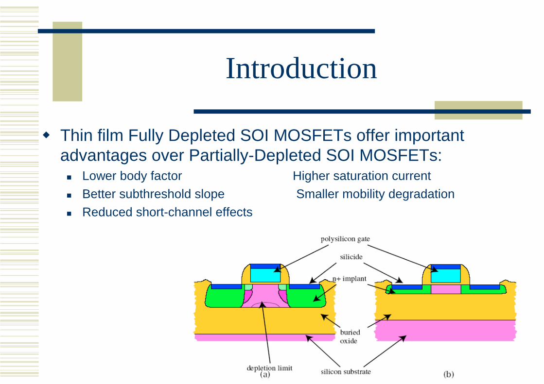
Introduction
� Thin film Fully Depleted SOI MOSFETs offer important advantages over Partially-Depleted SOI MOSFETs:� Lower body factor Higher saturation current� Better subthreshold slope Smaller mobility degradation� Reduced short-channel effects

MOS-AK September 2008 B. Iñiguez 6
Introduction
� The non-classical multi-gate devices such as Double-Gate (DG) MOSFETs, FinFETs or Gate-All-Around (GAA) MOSFETs show an even stronger control of short channel effects, and increase of on-currents taking advantage of volume inversion/accumulation.
DG MOSFET GAA MOSFET FinFET
MOS-AK September 2008 B. Iñiguez 7
Introduction
� The availability of accurate compact models of Multiple-GateMOSFETs in integrated circuits is critical for the futuredesign ofcircuits using those devices
� Circuit design requires a complete small-signal model, withanalytical or semi-analytical expressions of:� Current
� Total charges
� Transconductance and conductance
� Transcapacitances
MOS-AK September 2008 B. Iñiguez 8
General Electrostatics
� The good electrostatic control of the channel by the gate in ultrathin bodyMOSFETs (full depletion in subthreshold, i.e., no punchtrough) allows to use undoped or lightly-doped Si bodies. Mobility is higher in undoped bodies thanin doped ones.
� In ultrathin body MOSFETs, a proper description of the electrostatics should take into account the effects of both dopants and charge carriers.
� In FD SOI MOSFETs the Si film is fully depleted, while the front and back interface can be inverted, depleted or accumulated� The practical case is: front interface inverted and back interface accumulated
� In Multi-Gate MOSFETs, the Si body can be fully inverted or accumulated (volume inversion or accumulation)
MOS-AK September 2008 B. Iñiguez 9
General Electrostatics
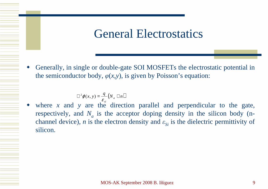
� Generally, in single or double-gate SOI MOSFETs the electrostatic potential in the semiconductor body, φ(x,y), is given by Poisson’s equation:
� where x and y are the direction parallel and perpendicular to the gate, respectively, and Na is the acceptor doping density in the silicon body (n-channel device), n is the electron density and εSi is the dielectric permittivity of silicon.
( )nNq
yx asi
+=∇ε
ϕ ),(2
MOS-AK September 2008 B. Iñiguez 10
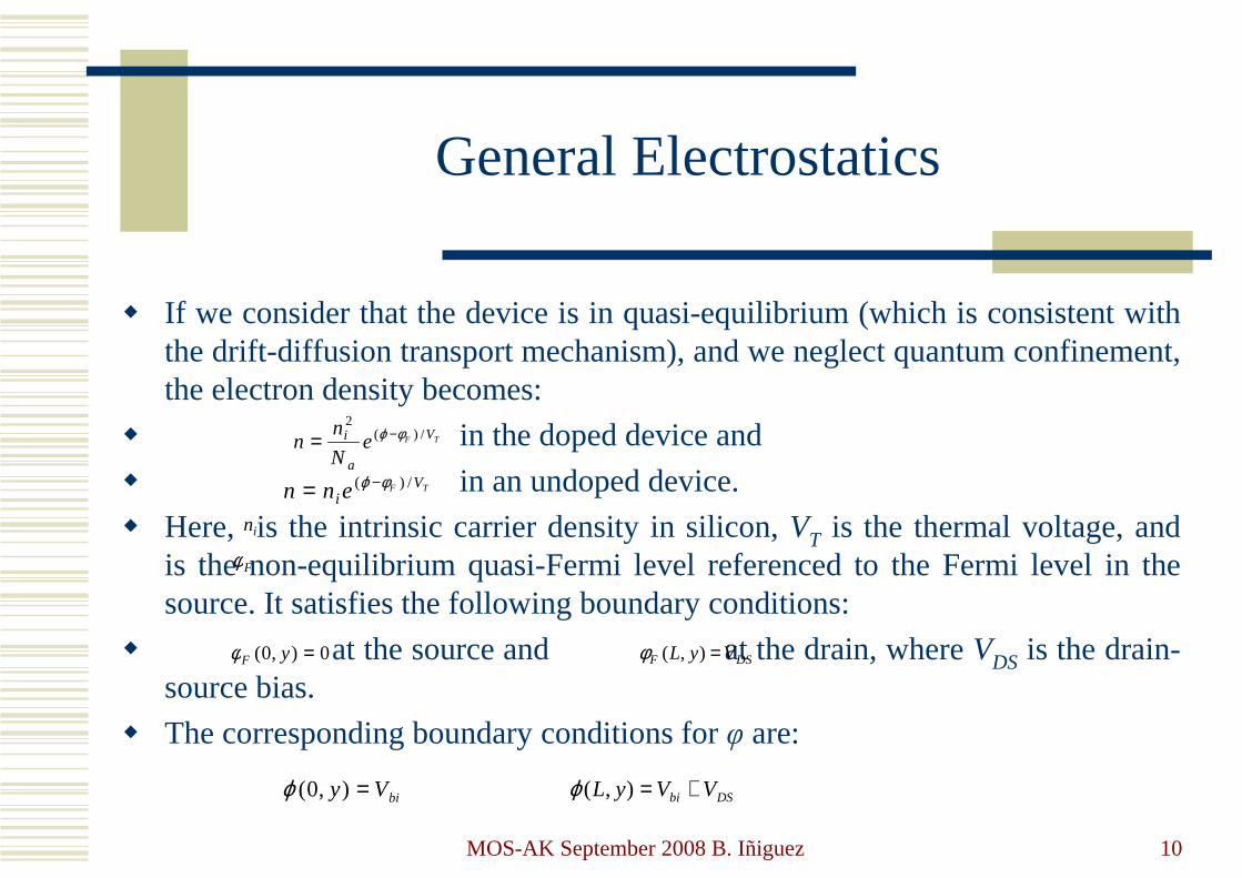
General Electrostatics
� If we consider that the device is in quasi-equilibrium (which is consistent with the drift-diffusion transport mechanism), and we neglect quantum confinement, the electron density becomes:
� in the doped device and
� in an undoped device.
� Here, is the intrinsic carrier density in silicon, VT is the thermal voltage, and is the non-equilibrium quasi-Fermi level referenced to the Fermi level in the source. It satisfies the following boundary conditions:
� at the source and at the drain, where VDS is the drain-source bias.
� The corresponding boundary conditions for φ are:
TF V
a
i eN
nn /)(
2φϕ −=
TF Vi enn /)( φϕ −=
in
Fφ
0),0( =yFφ DSF VyL =),(φ
biVy =),0(ϕ DSbi VVyL +=),(ϕ
MOS-AK September 2008 B. Iñiguez 11
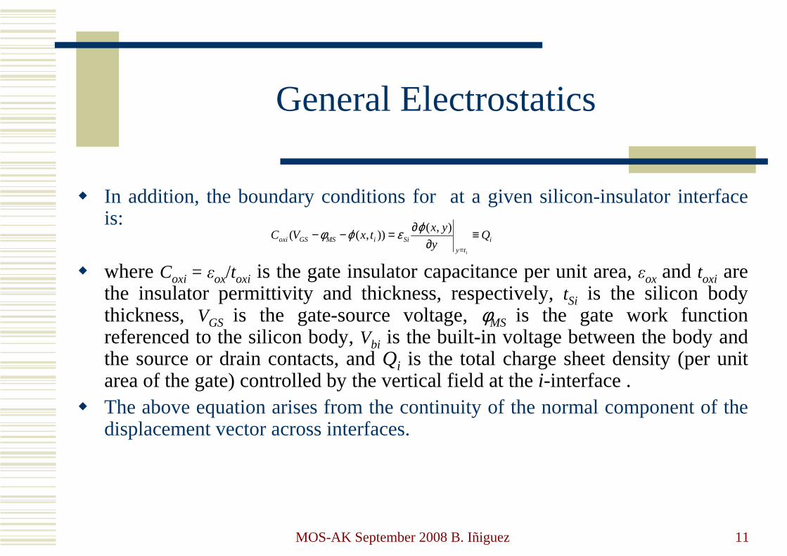
General Electrostatics
� In addition, the boundary conditions for at a given silicon-insulator interface is:
� where Coxi = εox/toxi is the gate insulator capacitance per unit area, εox and toxi are the insulator permittivity and thickness, respectively, tSi is the silicon body thickness, VGS is the gate-source voltage, φMS is the gate work function referenced to the silicon body, Vbi is the built-in voltage between the body and the source or drain contacts, and Qi is the total charge sheet density (per unit area of the gate) controlled by the vertical field at the i-interface .
� The above equation arises from the continuity of the normal component of the displacement vector across interfaces.
i
ty
SiiMSGSoxi Qy
yxtxVC
i
≡∂
∂=−−=
),()),((
ϕεϕφ
MOS-AK September 2008 B. Iñiguez 12
General Electrostatics
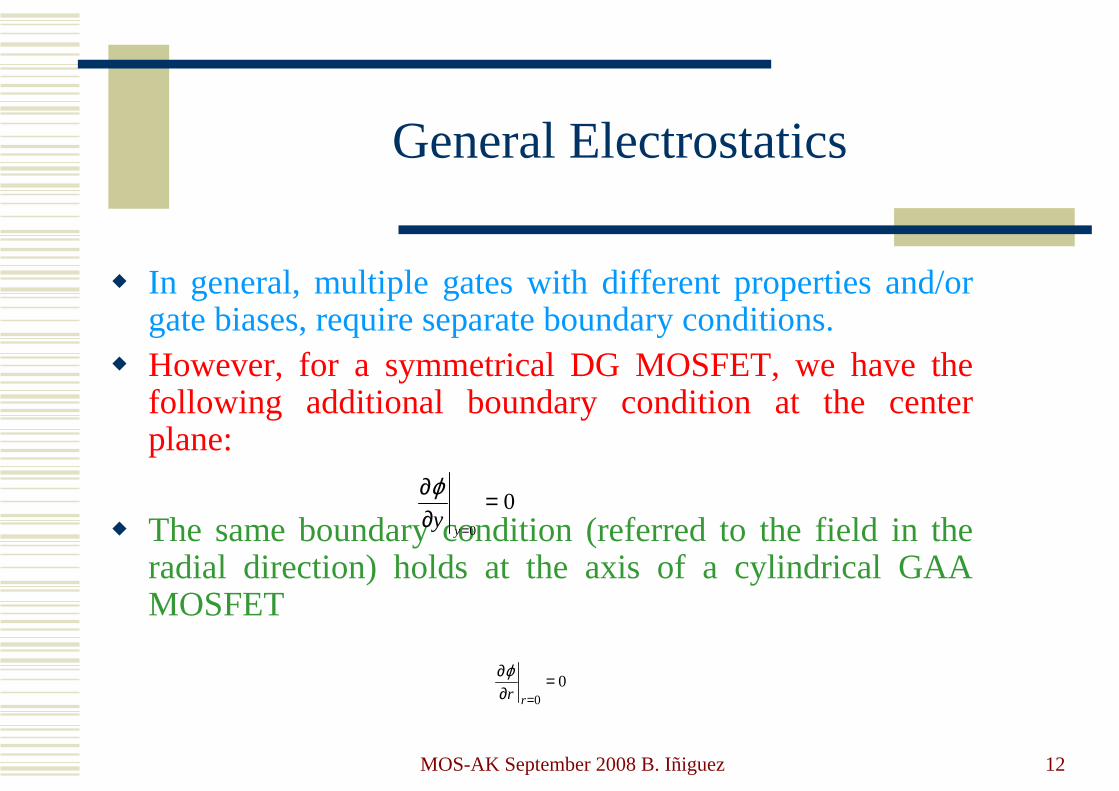
� In general, multiple gates with different properties and/or gate biases, require separate boundary conditions.
� However, for a symmetrical DG MOSFET, we have the following additional boundary condition at the center plane:
� The same boundary condition (referred to the field in the radial direction) holds at the axis of a cylindrical GAA MOSFET
00
=∂∂
=yy
ϕ
00
=∂∂
=rr
ϕ
MOS-AK September 2008 B. Iñiguez 13
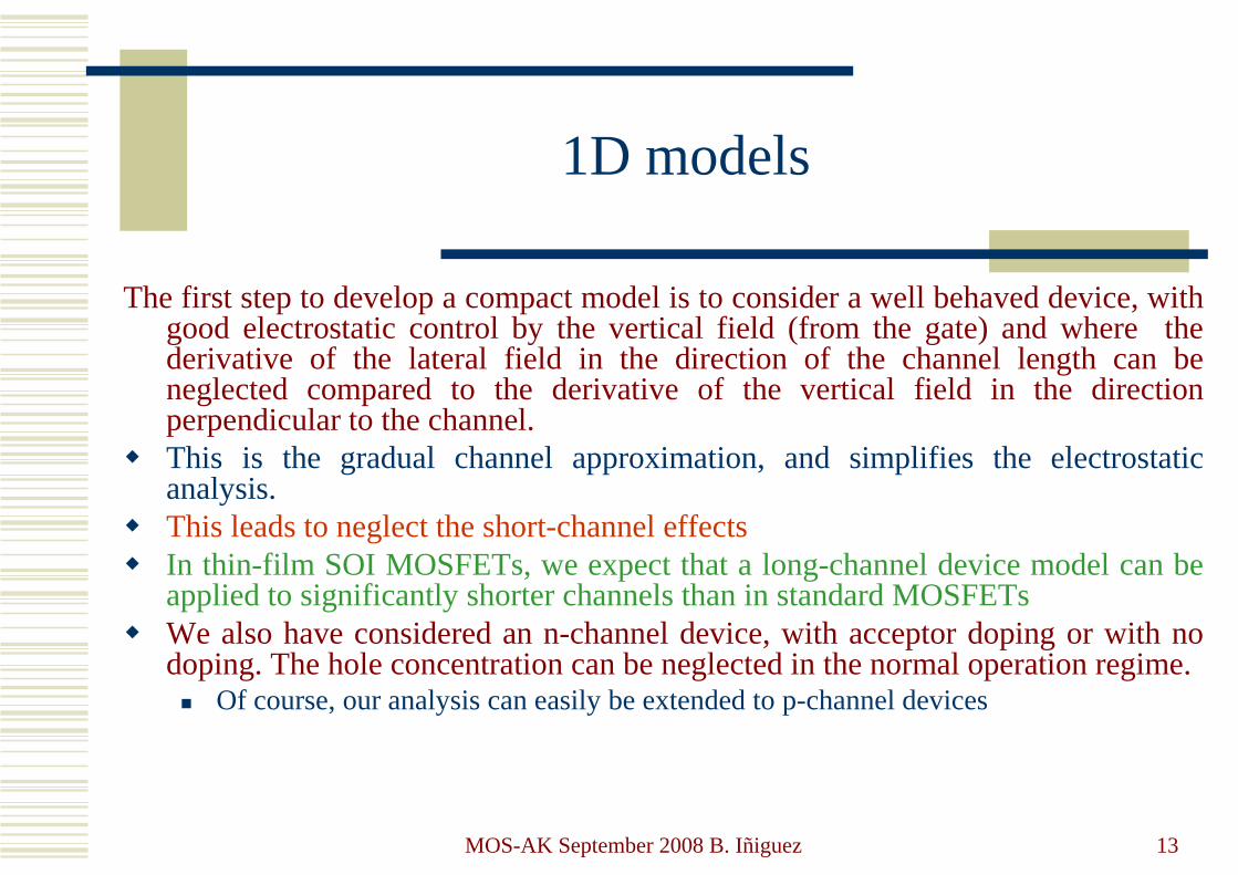
1D models
The first step to develop a compact model is to consider a well behaved device, with good electrostatic control by the vertical field (from the gate) and where the derivative of the lateral field in the direction of the channel length can be neglected compared to the derivative of the vertical field in the direction perpendicular to the channel.
� This is the gradual channel approximation, and simplifies the electrostatic analysis.
� This leads to neglect the short-channel effects� In thin-film SOI MOSFETs, we expect that a long-channel device model can be
applied to significantly shorter channels than in standard MOSFETs� We also have considered an n-channel device, with acceptor doping or with no
doping. The hole concentration can be neglected in the normal operation regime.� Of course, our analysis can easily be extended to p-channel devices
MOS-AK September 2008 B. Iñiguez 14
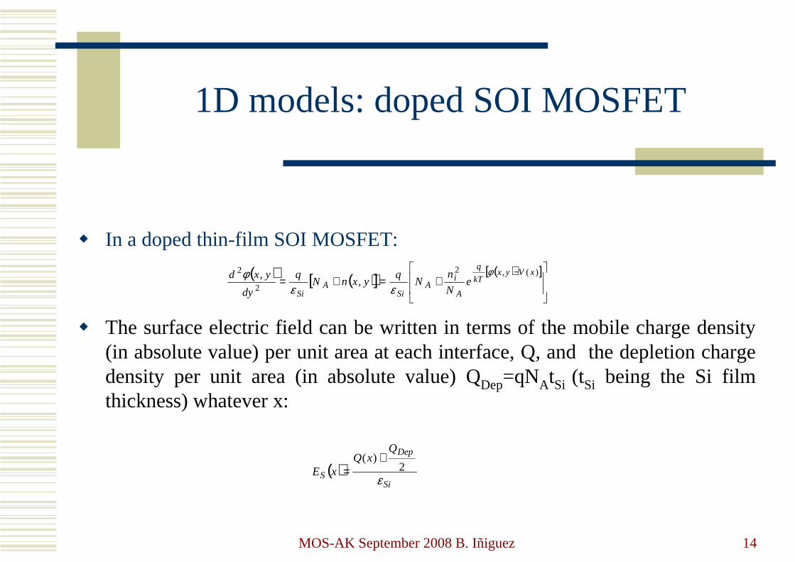
1D models: doped SOI MOSFET
� In a doped thin-film SOI MOSFET:
� The surface electric field can be written in terms of the mobile charge density (in absolute value) per unit area at each interface, Q, and the depletion charge density per unit area (in absolute value) QDep=qNAtSi (tSi being the Si film thickness) whatever x:
( ) ( )[ ]( )[ ]
+=+=
− )(,2
2
2,
, xVyxkT
q
A
iA
SiA
Sie
N
nN
qyxnN
q
dy
yxd φ
εεφ
( )Si
Dep
S
QxQ
xEε
2)( +
=
MOS-AK September 2008 B. Iñiguez 15
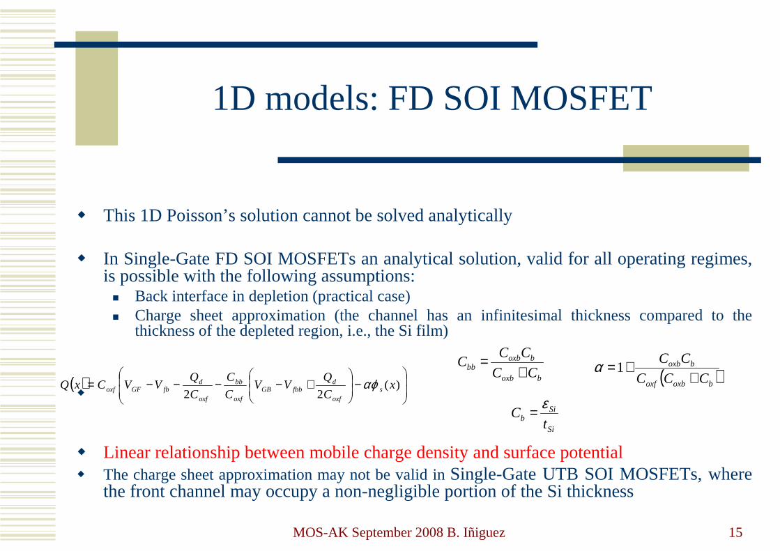
1D models: FD SOI MOSFET
� This 1D Poisson’s solution cannot be solved analytically
� In Single-Gate FD SOI MOSFETs an analytical solution, valid for all operating regimes, is possible with the following assumptions:� Back interface in depletion (practical case)� Charge sheet approximation (the channel has an infinitesimal thickness compared to the
thickness of the depleted region, i.e., the Si film)
�
� Linear relationship between mobile charge density and surface potential� The charge sheet approximation may not be valid in Single-Gate UTB SOI MOSFETs, where
the front channel may occupy a non-negligible portion of the Si thickness
( )
−
+−−−−= )(
22x
C
QVV
C
C
C
QVVCxQ s
oxf
dfbbGB
oxf
bb
oxf
dfbGFoxf αϕ boxb
boxbbb CC
CCC
+=
( )boxboxf
boxb
CCC
CC
++=1α
Si
Sib t
Cε=
MOS-AK September 2008 B. Iñiguez 16
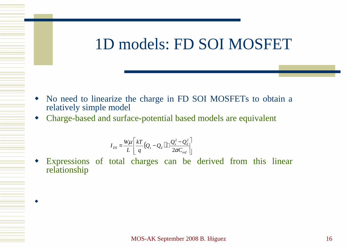
1D models: FD SOI MOSFET
� No need to linearize the charge in FD SOI MOSFETs to obtain a relatively simple model
� Charge-based and surface-potential based models are equivalent
� Expressions of total charges can be derived from this linear relationship
�
( )
−+−=oxf
dsdsDS C
QQQQ
q
kT
L
WI
αµ
2
22
MOS-AK September 2008 B. Iñiguez 17
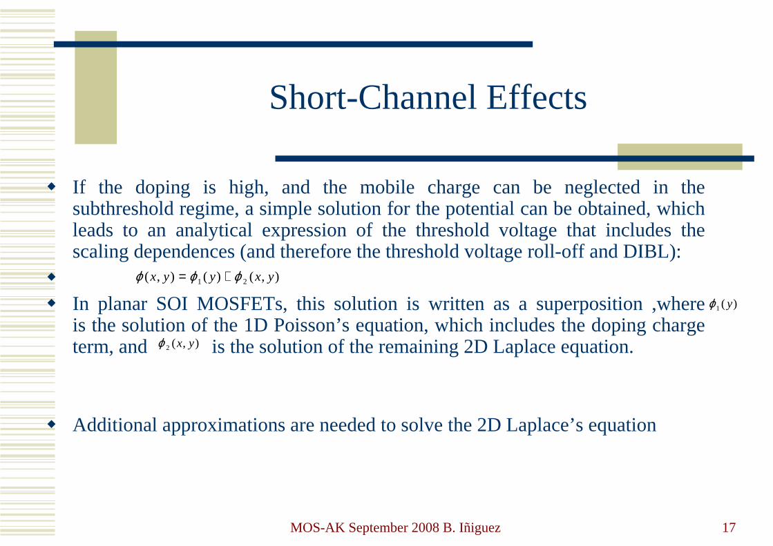
Short-Channel Effects
� If the doping is high, and the mobile charge can be neglected in the subthreshold regime, a simple solution for the potential can be obtained, which leads to an analytical expression of the threshold voltage that includes the scaling dependences (and therefore the threshold voltage roll-off and DIBL):
�
� In planar SOI MOSFETs, this solution is written as a superposition ,where is the solution of the 1D Poisson’s equation, which includes the doping charge term, and is the solution of the remaining 2D Laplace equation.
� Additional approximations are needed to solve the 2D Laplace’s equation
),()(),( 21 yxyyx ϕϕϕ +=
)(1 yϕ
),(2 yxϕ
MOS-AK September 2008 B. Iñiguez 18
Short-Channel Effects
� In FD SOI MOSFETs the 2D Poisson’s equation in subthreshold can by solved by neglecting the mobile charge density, which is much lower than the doped charge density
� An analytical expression of the threshold voltage, that takes into account the scaling dependencies, the roll-off and the DIBL can be obtained from that solution after using several approximations and a few adjustable parameters (quasi-2D model). The electrostatic short-channel effects are accounted for (in many models) by means of the threshold voltage expression, which is used in the drain current expression derived for long-channel devices
� Standard FD SOI MOSFET models take into account the short-channel effects using this approach
MOS-AK September 2008 B. Iñiguez 19
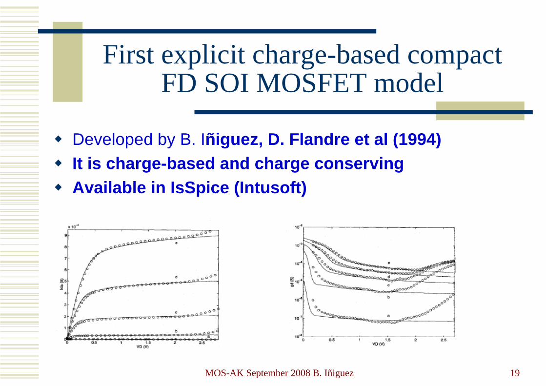
First explicit charge-based compact FD SOI MOSFET model
� Developed by B. Iñiguez, D. Flandre et al (1994)� It is charge-based and charge conserving� Available in IsSpice (Intusoft)
MOS-AK September 2008 B. Iñiguez 20
Standard Models of FD SOI MOSFETs
� BSIMSOI
� UFSOI
� HiSIM-SOI
MOS-AK September 2008 B. Iñiguez 21
BSIMSOI
� Developed as an extension of a bulk MOSFET model� It extends a strong inversion explicit model by using proper interpolation
functions� It includes a smooth transition between the PD and the FD regime
(Dynamically Depleted SOI MOSFET)� Temperature dependence of threshold voltage, mobility, saturation velocity,
parasitic resistance, and diode currents
� Different gate resistance options for RF simulation:� Intrinsic input gate resistance, reflected to the gate from the intrinsic channel
region. It is bias dependent and a first-order non-quasi static model, for RF and rapid transientMOSFET operations
� Last version: BSIMSOI 4.0: addresses several new issues in modeling sub-0.13 micron CMOS/SOI high-speed and RF circuit simulation.
MOS-AK September 2008 B. Iñiguez 22
BSIMSOI
� Improvements of BSIM 4.0:� Asymmetric current/capacitance model S/D diode and asymmetric S/D resistance; � Improved GIDL model with BSIM4 GIDL compatibility� Noise model Improvements;
� Improved width/length dependence on flicker noise � SPICE2 thermal noise model is introduced as TNOIMOD=2 with parameter NTNOI that adjusts the
magnitude of the noise density � Body contact resistance induced thermal noise � Thermal noise induced by the body resistance network � Shot noises induced by Ibs and Ibd separated
� A two resistance body resistance network introduced for RF simulation; � Threshold voltage model enhancement;
� Long channel DIBL effect model added � Channel-length dependence of body effect improved
� Drain induced threshold shift(DITS) model introduced in output conductance; � Improved model accuracy in moderate inversion region with BSIM4 compatible Vgsteff;
MOS-AK September 2008 B. Iñiguez 23
FD/SOI UFSOI
� The University of Florida developed one model for PD SOI MOSFETs (UFPDB) and one model for FD SOI MOSFETS (FD/SOI UFSOI)
� It is charge-based, and considers 5 terminals� It is strongly physically-based, and needs iterations� The model accounts for the charge coupling between the front and back gates� It includes a two-dimensional analysis of the electrostatic potential in the SOI film
and underlying BOX for subthreshold-region operation. � The model assumes that the film is strongly FD, except in and near the
accumulation region where it accounts for the majority-carrier charge, and hence dynamic floating-body effects.
� Two dimensional analysis for weak-inversion current� Spline interpolations of current and charge across a physically defined,
bias-dependent moderate-inversion region linking the weak- and strong-inversion formalisms
MOS-AK September 2008 B. Iñiguez 24
FD/SOI UFSOI
� Temperature dependence is also implemented, without the need for any additional parameters
� Physics-based noise modeling for AC simulation, which accounts for thermal noise from the channel and parasitic series rresistances, shot noise at the source and drain junctions, and flicker noise in the channel.
� The temperature-dependence modeling is the basis for a self-heating option, which uses special iterate control for the local device temperature node.
� Because of the process basis of the models, parameter evaluation can be based in part on device structure
� Option for a strained Si/SiGe channel.
MOS-AK September 2008 B. Iñiguez 25
HiSIM SOI
� Based on a complete surface-potential description. � The surface potential in the MOSFET channel, and the potentials at both
surfaces of the buried oxide� This allows to include all relevant device features of the SOI-MOSFET� An additional parasitic electric field, induced by the surface-potential
distribution at the buried oxide, has to be included for accurate modelingof the short-channel effects.
� It seems to have better convergence properties than BSIMSOI and UFSOI� It includes a 1/f noise model
MOS-AK September 2008 B. Iñiguez 26
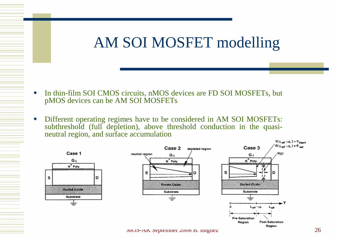
AM SOI MOSFET modelling
� In thin-film SOI CMOS circuits, nMOS devices are FD SOI MOSFETs, but pMOS devices can be AM SOI MOSFETs
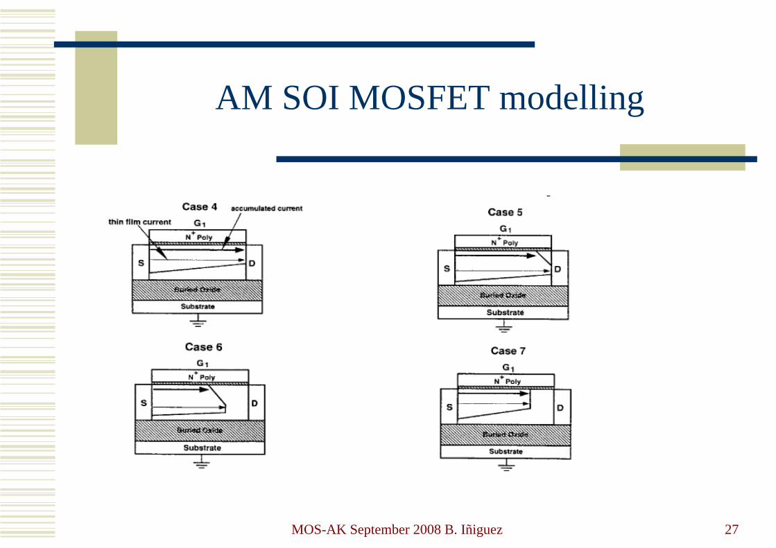
� Different operating regimes have to be considered in AM SOI MOSFETs: subthreshold (full depletion), above threshold conduction in the quasi-neutral region, and surface accumulation
�
MOS-AK September 2008 B. Iñiguez 27
AM SOI MOSFET modelling
MOS-AK September 2008 B. Iñiguez 28
AM SOI MOSFET modelling
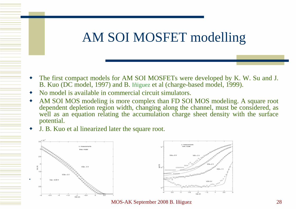
� The first compact models for AM SOI MOSFETs were developed by K. W. Su and J. B. Kuo (DC model, 1997) and B. Iñiguezet al (charge-based model, 1999).
� No model is available in commercial circuit simulators.� AM SOI MOS modeling is more complex than FD SOI MOS modeling. A square root
dependent depletion region width, changing along the channel, must be considered, as well as an equation relating the accumulation charge sheet density with the surface potential.
� J. B. Kuo et al linearized later the square root.
�
MOS-AK September 2008 B. Iñiguez 29
AM SOI MOSFET modelling
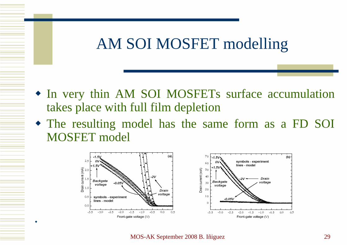
� In very thin AM SOI MOSFETs surface accumulation takes place with full film depletion
� The resulting model has the same form as a FD SOI MOSFET model
�
MOS-AK September 2008 B. Iñiguez 30
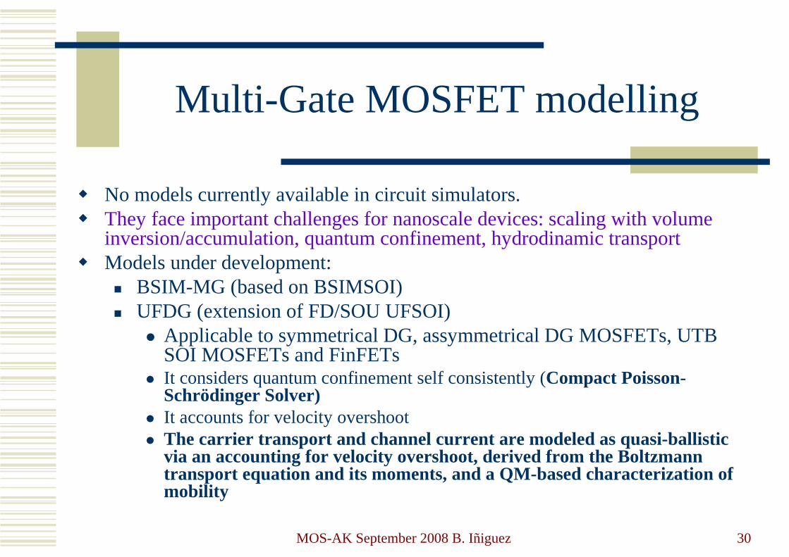
Multi-Gate MOSFET modelling
� No models currently available in circuit simulators.� They face important challenges for nanoscale devices: scaling with volume
inversion/accumulation, quantum confinement, hydrodinamic transport� Models under development:
� BSIM-MG (based on BSIMSOI)� UFDG (extension of FD/SOU UFSOI)
� Applicable to symmetrical DG, assymmetrical DG MOSFETs, UTB SOI MOSFETs and FinFETs
� It considers quantum confinement self consistently (Compact Poisson-Schrödinger Solver)
� It accounts for velocity overshoot� The carrier transport and channel current are modeled as quasi-ballistic
via an accounting for velocity overshoot, derived from the Boltzmann transport equation and its moments, and a QM-based characterization of mobility
MOS-AK September 2008 B. Iñiguez 31
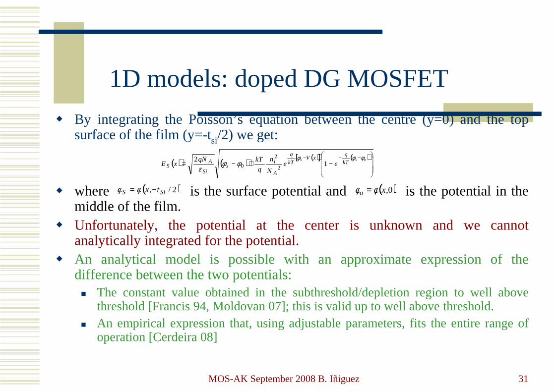
1D models: doped DG MOSFET
� By integrating the Poisson’s equation between the centre (y=0) and the top surface of the film (y=-tsi/2) we get:
� where is the surface potential and is the potential in the middle of the film.
� Unfortunately, the potential at the center is unknown and we cannot analytically integrated for the potential.
� An analytical model is possible with an approximate expression of the difference between the two potentials:� The constant value obtained in the subthreshold/depletion region to well above
threshold [Francis 94, Moldovan 07]; this is valid up to well above threshold.� An empirical expression that, using adjustable parameters, fits the entire range of
operation [Cerdeira 08]
( ) ( )( )[ ] ( )
−+−=
−−− 0
12
2
2
0
φφφφφ
εsS kT
qxV
kT
q
A
is
Si
AS ee
N
n
q
kTqNxE
( )2/, SiS tx −= φφ ( )0,xo φφ =
MOS-AK September 2008 B. Iñiguez 32
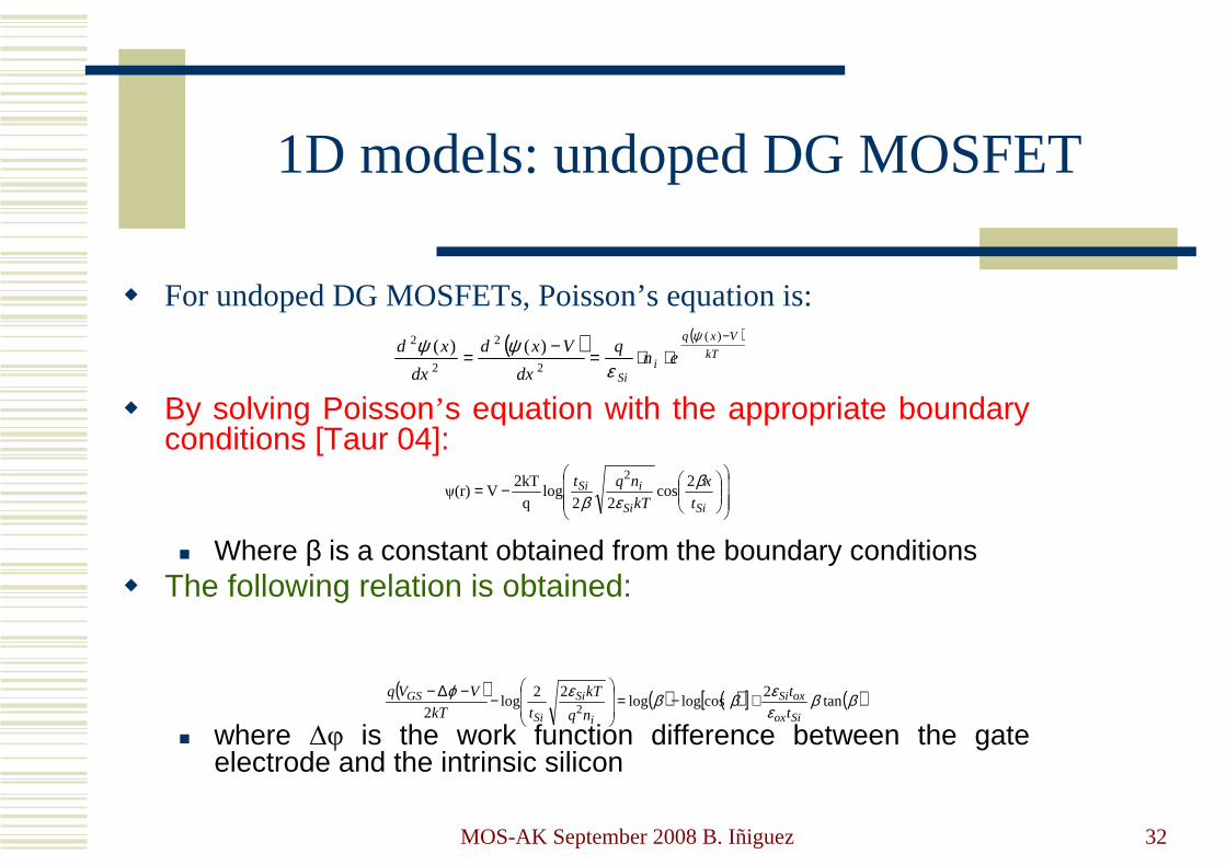
1D models: undoped DG MOSFET
� For undoped DG MOSFETs, Poisson’s equation is:
� By solving Poisson’s equation with the appropriate boundary conditions [Taur 04]:
� Where β is a constant obtained from the boundary conditions� The following relation is obtained:
� where ∆φ is the work function difference between the gate electrode and the intrinsic silicon
−=
SiSi
iSi
t
x
kT
nqt βεβ
2cos
22log
q
2kTVψ(r)
2
( ) ( )kT
Vxq
iSi
enq
dx
Vxd
dx
xd−
⋅⋅=−
=)(
2
2
2
2 )()(ψ
εψψ
( ) ( ) ( )[ ] ( )ββεεββεϕ
tan2
cosloglog22
log2 2
Siox
oxSi
i
Si
Si
GS
t
t
nq
kT
tkT
VVq +−=
−−∆−
MOS-AK September 2008 B. Iñiguez 33
1D models: undoped DG MOSFET
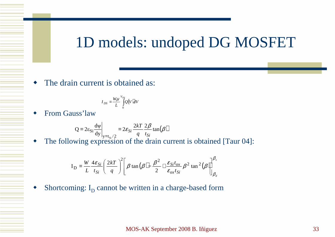
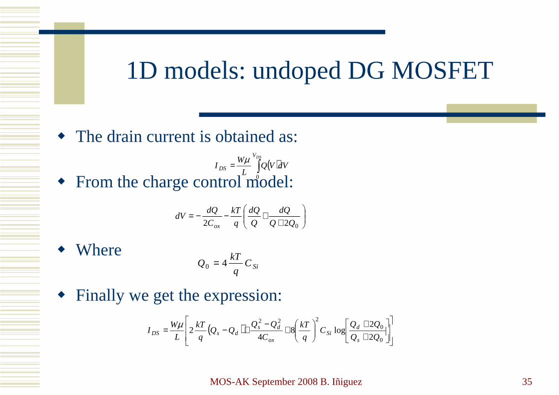
� The drain current is obtained as:
� From Gauss’law
� The following expression of the drain current is obtained [Taur 04]:
� Shortcoming: ID cannot be written in a charge-based form
( )∫=DSV
DS dVVQL
WI
0
µ
( )ββε tan22
2dy
dψε2Q
2/tySi
SiSi
Si tq
kT===
( ) ( )s
dSiox
oxSi
Si
Si
t
t
q
kT
tL
Wβ
β
ββεεβββε
+−
= 22
22
D tan2
tan24
I
MOS-AK September 2008 B. Iñiguez 34
1D models: undoped DG MOSFET
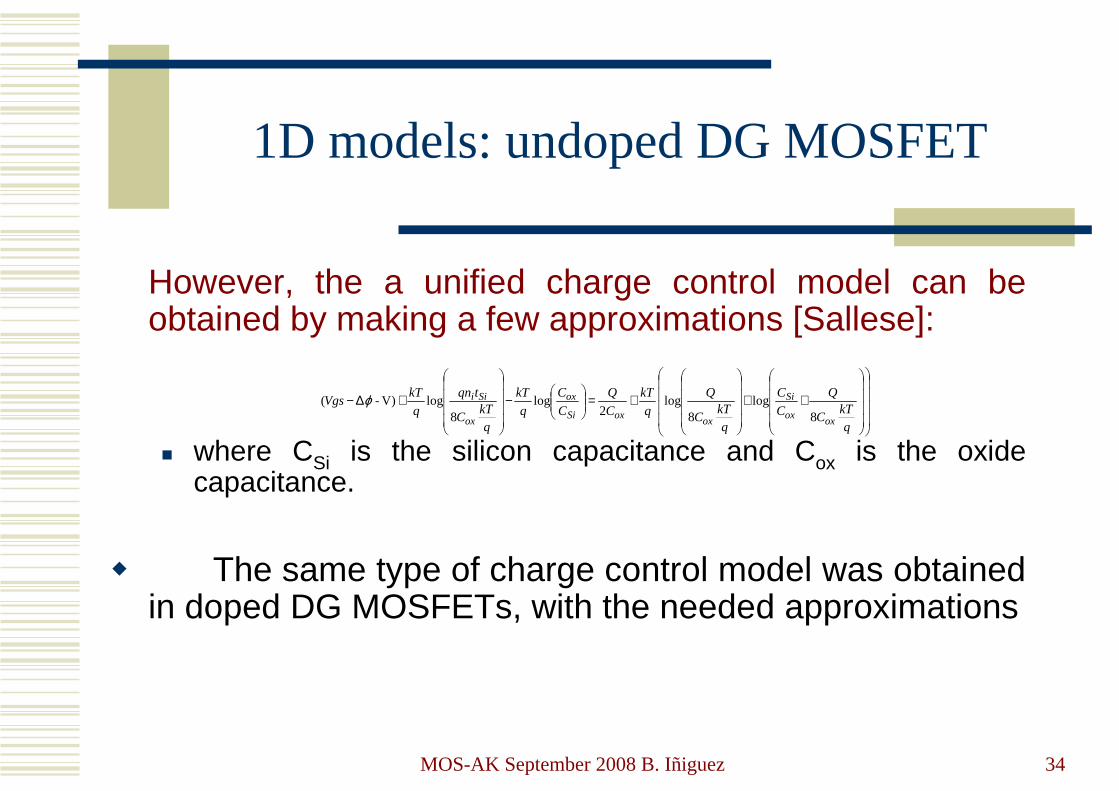
However, the a unified charge control model can be obtained by making a few approximations [Sallese]:
� where CSi is the silicon capacitance and Cox is the oxide capacitance.
� The same type of charge control model was obtained in doped DG MOSFETs, with the needed approximations
++
+=
−
+∆−
qkT
C
Q
C
C
qkT
C
Q
q
kT
C
Q
C
C
q
kT
qkT
C
tqn
q
kTVgs
oxox
Si
oxoxSi
ox
ox
Sii
8log
8log
2log
8log)V-( ϕ
MOS-AK September 2008 B. Iñiguez 35
1D models: undoped DG MOSFET
� The drain current is obtained as:
� From the charge control model:
� Where
� Finally we get the expression:
( )∫=DSV
DS dVVQL
WI
0
µ
++−−=
022 QQ
dQ
Q
dQ
q
kT
C
dQdV
ox
( )
++
+
−+−=
0
0222
2
2log8
42
QQC
q
kT
C
QQQQ
q
kT
L
WI
s
dSi
ox
dsdsDS
µ
SiCq
kTQ 40 =
MOS-AK September 2008 B. Iñiguez 36
1D models: Cylindrical GAA MOSFET
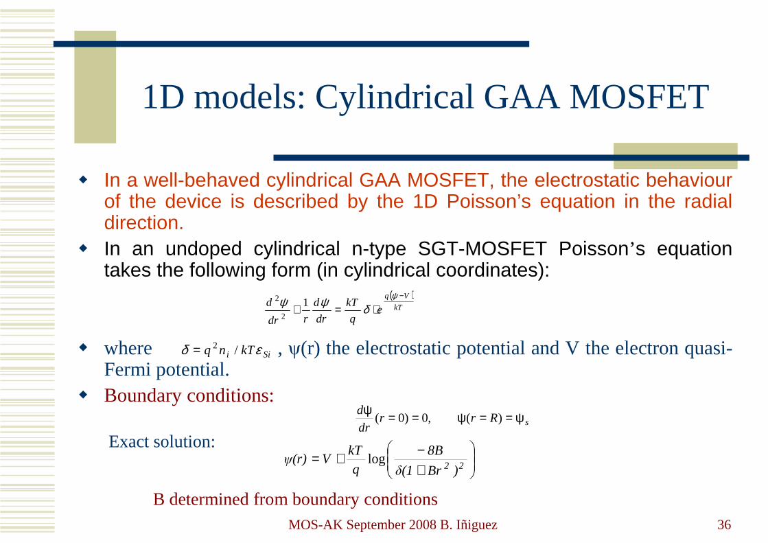
� In a well-behaved cylindrical GAA MOSFET, the electrostatic behaviour of the device is described by the 1D Poisson’s equation in the radial direction.
� In an undoped cylindrical n-type SGT-MOSFET Poisson’s equation takes the following form (in cylindrical coordinates):
� where , ψ(r) the electrostatic potential and V the electron quasi-Fermi potential.
� Boundary conditions:
Exact solution:
B determined from boundary conditions
( )kT
Vq
eq
kT
dr
d
rdr
d−
⋅=+ψ
δψψ 12
2
Sii kTnq εδ /2=
sRrrdr
d ψ==ψ==ψ)(,0)0(
+−+=
22 )Brδ(1
8B
q
kTVψ(r) log
MOS-AK September 2008 B. Iñiguez 37
1D models: Cylindrical GAA MOSFET
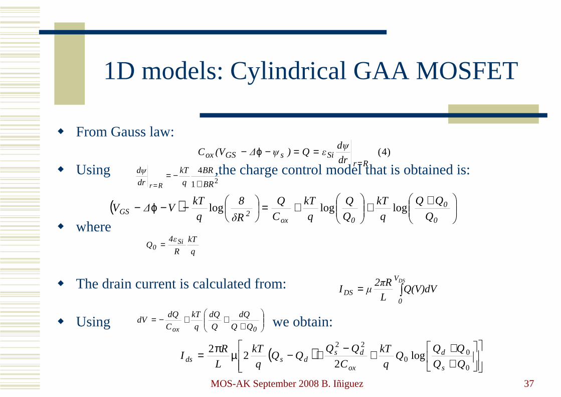
� From Gauss law:
� Using ,the charge control model that is obtained is:
� where
� The drain current is calculated from:
� Using we obtain:
)4(Rr
SisGSox dr
dψεQ)ψ∆(VC
===−ϕ−
21
4
BR
BR
q
kT
dr
dψ
Rr +−=
=
( )
++
+=
−−ϕ−0
0
0ox2GS Q
q
kT
Q
Q
q
kT
C
Q
δR
8
q
kTV∆V logloglog
q
kT
R
4εQ Si
0 =
∫=DSV
0DS Q(V)dV
L
R2πµI
( )
+++−+−µπ=
0
00
22
log2
22
QQQ
q
kT
C
QQQQ
q
kT
L
RI
s
d
ox
dsdsds
+++−=
0ox QQ
dQ
Q
dQ
q
kT
C
dQdV
MOS-AK September 2008 B. Iñiguez 38
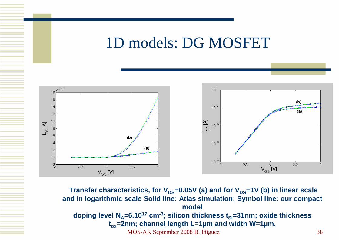
1D models: DG MOSFET
Transfer characteristics, for V DS=0.05V (a) and for V DS=1V (b) in linear scale and in logarithmic scale Solid line: Atlas simulati on; Symbol line: our compact
modeldoping level N A=6.1017 cm -3; silicon thickness t Si=31nm; oxide thickness
tox=2nm; channel length L=1µm and width W=1µm.
MOS-AK September 2008 B. Iñiguez 39
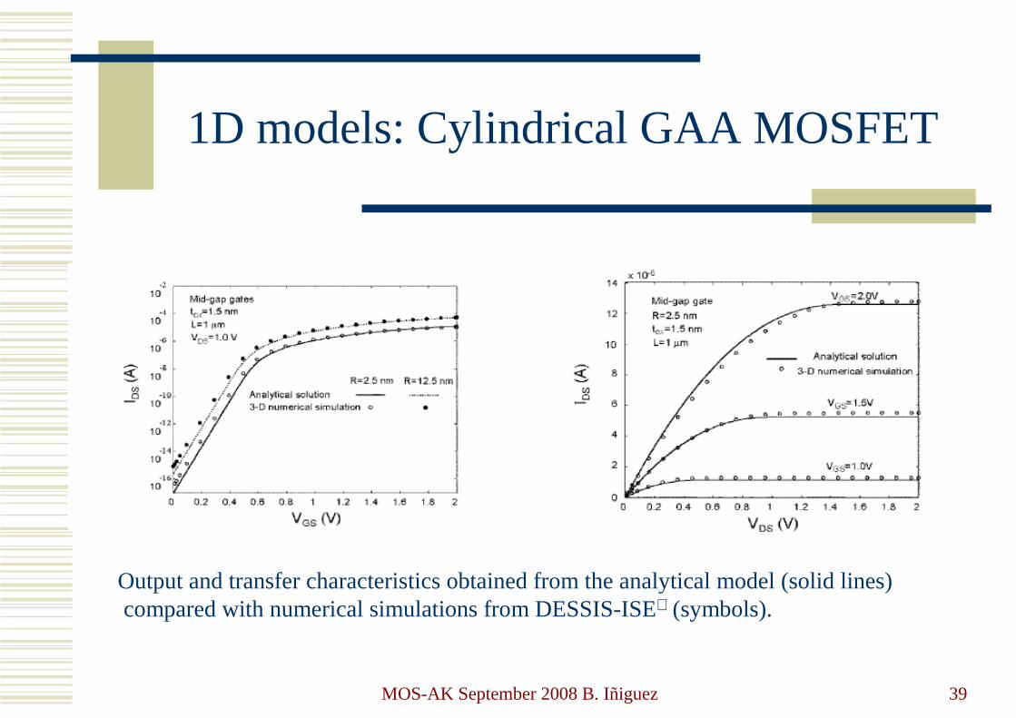
1D models: Cylindrical GAA MOSFET
Output and transfer characteristics obtained from the analytical model (solid lines)compared with numerical simulations from DESSIS-ISE (symbols).
MOS-AK September 2008 B. Iñiguez 40
1D models: FinFET
( )
++
+=−−−
0
0
0ox
0GS Q
QQlog
q
kT
Q
Qlog
q
kT
C
QVV V
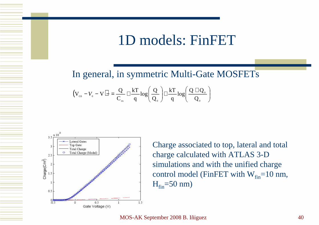
In general, in symmetric Multi-Gate MOSFETs
Charge associated to top, lateral and total charge calculated with ATLAS 3-D simulations and with the unified chargecontrol model (FinFET with Wfin=10 nm, Hfin=50 nm)
MOS-AK September 2008 B. Iñiguez 41
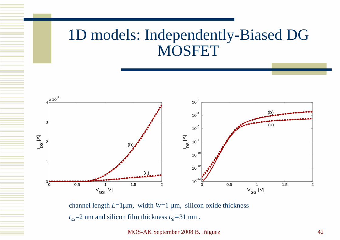
1D models: Independently-Biased DG MOSFET
� A similar unified charge control model is obtainedassuming the back interface in weak inversion, butwithout assuming the charge sheet approximation:
� Where
( )
( )
2
2 1
1 2
2
0 0
41 1 1log
1 1 1 1 2
1 2log log(2 ) log log 1
1 1
Si GS GB fb fb
GS GB fb fb
ox
ox
C V V v vkTV V V v v
kTq Cq
kT kT Q kT Q kT Qa
q q C q Q q Q
α αα α α α
αα α
− + − + − − − − ⋅ − + + + +
− − + = + + + + +
Si
Si ox
C
C Cα =
+ox
SiSi
Ct
ε= ( )0 2 14 Si GS fb fbQ C V v v= + − Si ox
ox D
ta
L
εε
= 2Si
Di
kTL
q n
ε=
MOS-AK September 2008 B. Iñiguez 42
1D models: Independently-Biased DG MOSFET
0 0.5 1 1.5 20
1
2
3
4x 10
-4
I DS [A
]
VGS
[V]
(a)
(b)
0 0.5 1 1.5 210
-14
10-12
10-10
10-8
10-6
10-4
10-2
I DS [A
]V
GS [V]
(a)
(b)
channel length L=1µm, width W=1 µm, silicon oxide thickness
tox=2 nm and silicon film thickness tSi=31 nm .
MOS-AK September 2008 B. Iñiguez 43
2D models Multi-Gate MOSFETs
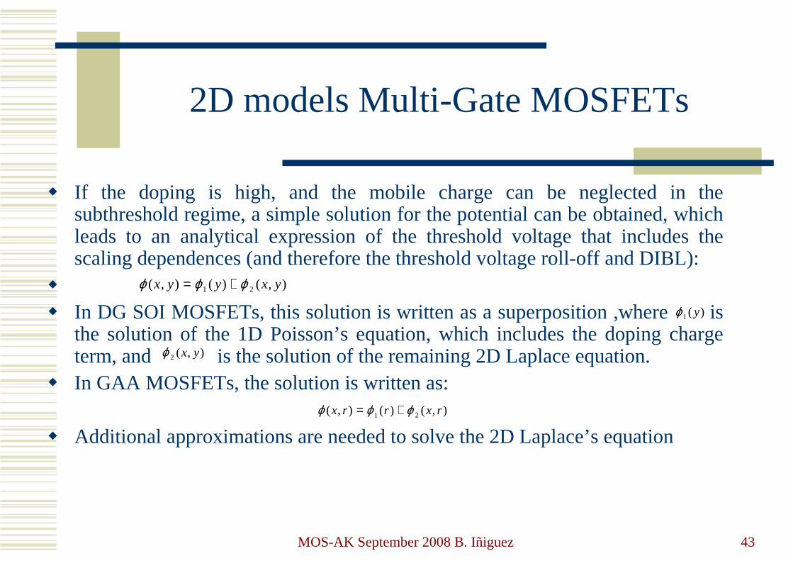
� If the doping is high, and the mobile charge can be neglected in the subthreshold regime, a simple solution for the potential can be obtained, which leads to an analytical expression of the threshold voltage that includes the scaling dependences (and therefore the threshold voltage roll-off and DIBL):
�
� In DG SOI MOSFETs, this solution is written as a superposition ,where is the solution of the 1D Poisson’s equation, which includes the doping charge term, and is the solution of the remaining 2D Laplace equation.
� In GAA MOSFETs, the solution is written as:
� Additional approximations are needed to solve the 2D Laplace’s equation
),()(),( 21 yxyyx ϕϕϕ +=
)(1 yϕ
),(2 yxϕ
),()(),( 21 rxrrx ϕϕϕ +=
MOS-AK September 2008 B. Iñiguez 44
2D models
� An analytical expression of the threshold voltage, that takes into account the scaling dependencies, the roll-off and the DIBL can be obtained from that solution after using several approximations and a few adjustable parameters (quasi-2D model). The electrostatic short-channel effects are accounted for (in many models) by means of the threshold voltage expression, which is used in the drain current expression
� More rigorous solutions (fully 2D or 3D models, or “predictive models”):
� Truncation of series of hyperbolic functions (DG MOSFETs, FinFETs), or Bessel functions (GAA MOSFETs)
� Conformal mapping
MOS-AK September 2008 B. Iñiguez 45
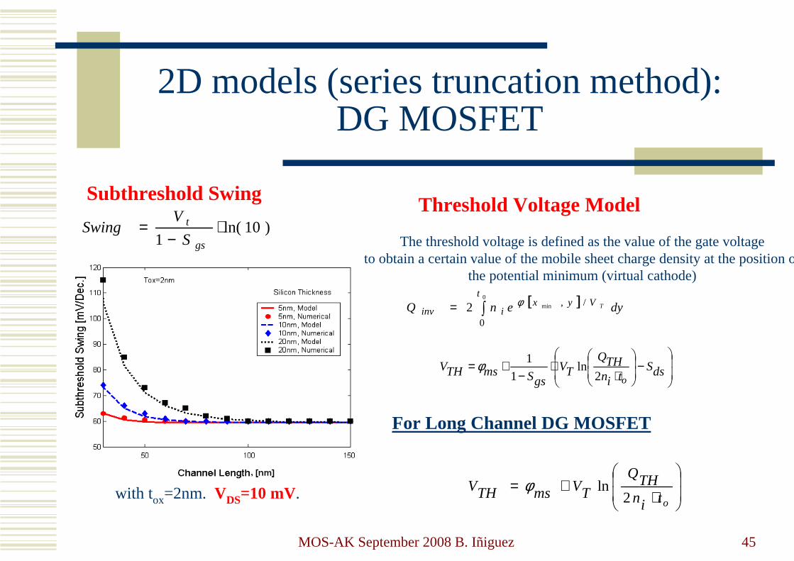
2D models (series truncation method): DG MOSFET
Subthreshold swing for DG MOSFETwith tox=2nm. VDS=10 mV.
)10ln(1
⋅−
=gs
t
S
VSwing
[ ]∫=0
min
0
/,2t
Vyxiinv dyenQ Tφ
The threshold voltage is defined as the value of the gate voltage to obtain a certain value of the mobile sheet charge density at the position of
the potential minimum (virtual cathode)
−
⋅⋅
−+= dsS
tinTHQ
TVgsSmsTHV
o2ln
1
1φ
⋅+=
otinTHQ
TVmsTHV2
lnφ
For Long Channel DG MOSFET
Subthreshold Swing Threshold Voltage Model
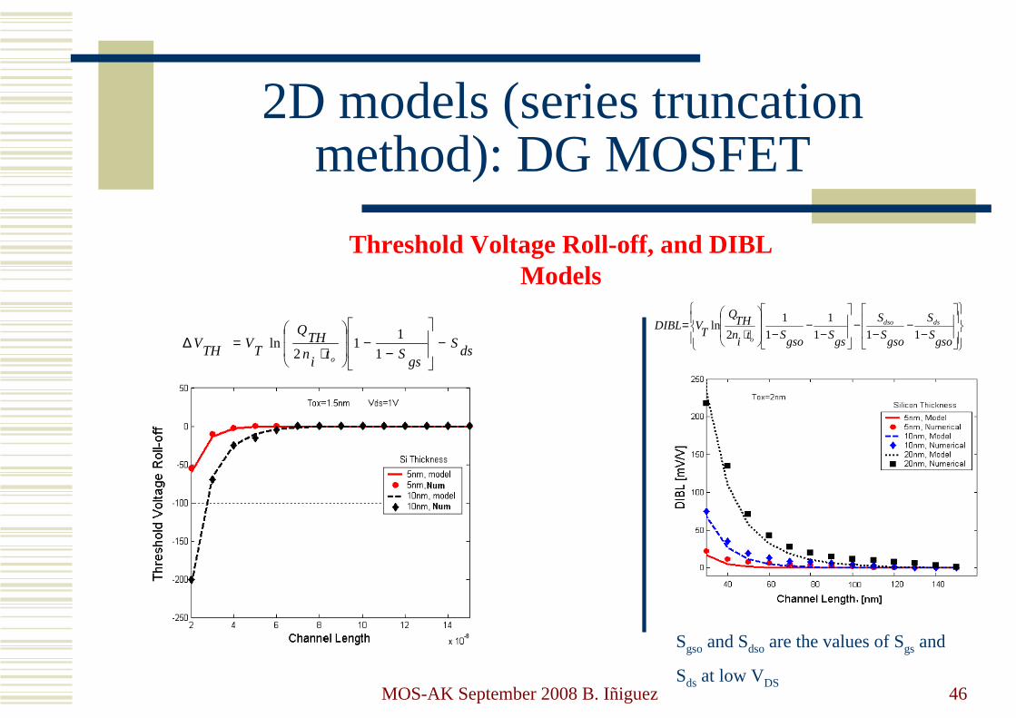
MOS-AK September 2008 B. Iñiguez 46
2D models (series truncationmethod): DG MOSFET
dsS
gsSt
inTH
Q
TV
THV
o
−
−−
⋅=∆
1
11
2ln
−−
−−
−−
−
⋅=
gsoS
S
gsoS
S
gsS
gsoSt
inTH
Q
TVDIBL dsdso
o 111
1
1
1
2ln
Threshold Voltage Roll-off, and DIBL Models
Sgsoand Sdsoare the values of Sgs and
Sds at low VDS
MOS-AK September 2008 B. Iñiguez 47
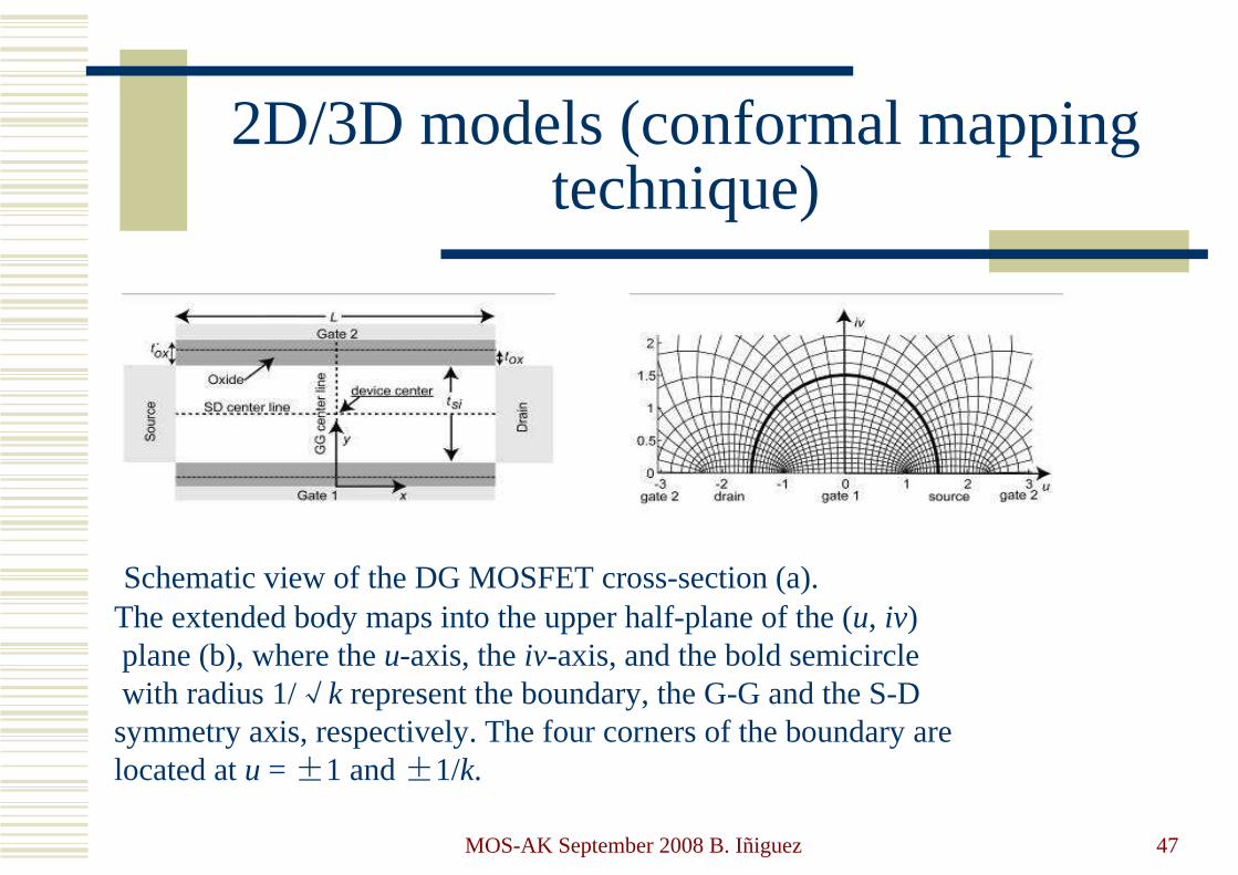
2D/3D models (conformal mappingtechnique)
Schematic view of the DG MOSFET cross-section (a). The extended body maps into the upper half-plane of the (u, iv)plane (b), where the u-axis, the iv-axis, and the bold semicirclewith radius 1/√k represent the boundary, the G-G and the S-D symmetry axis, respectively. The four corners of the boundary are located at u = ±1 and ±1/k.
MOS-AK September 2008 B. Iñiguez 48
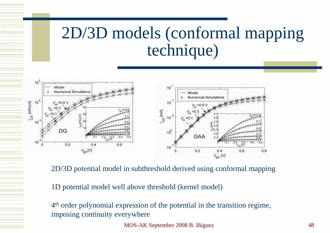
2D/3D models (conformal mappingtechnique)
2D/3D potential model in subthreshold derived using conformal mapping
1D potential model well above threshold (kernel model)
4th order polynomial expression of the potential in the transition regime, imposing continuity everywhere
MOS-AK September 2008 B. Iñiguez 49
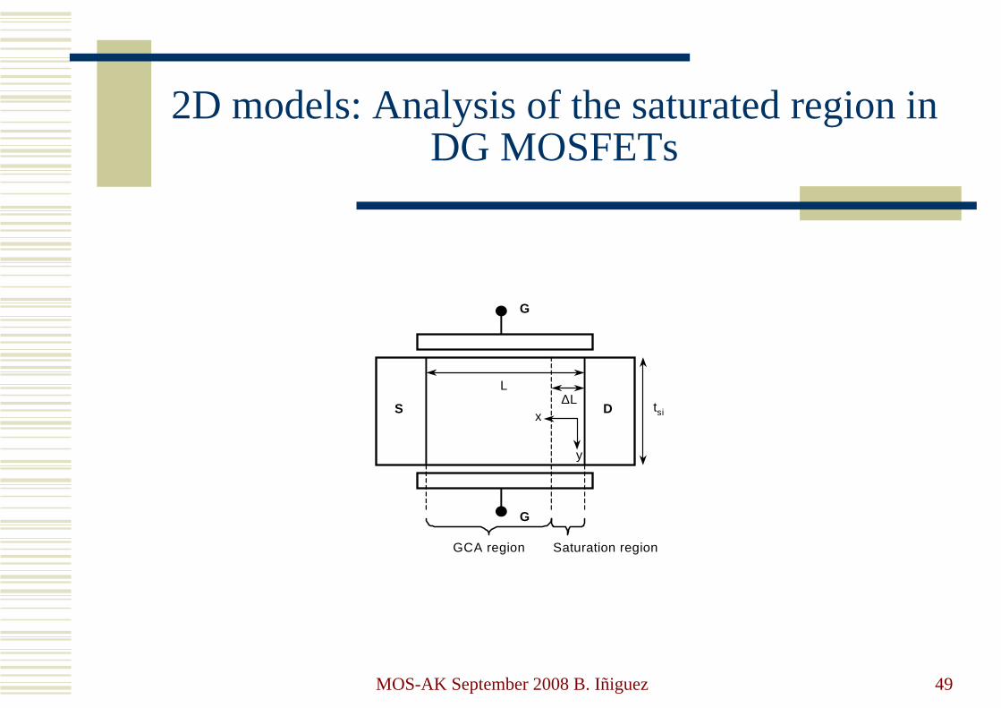
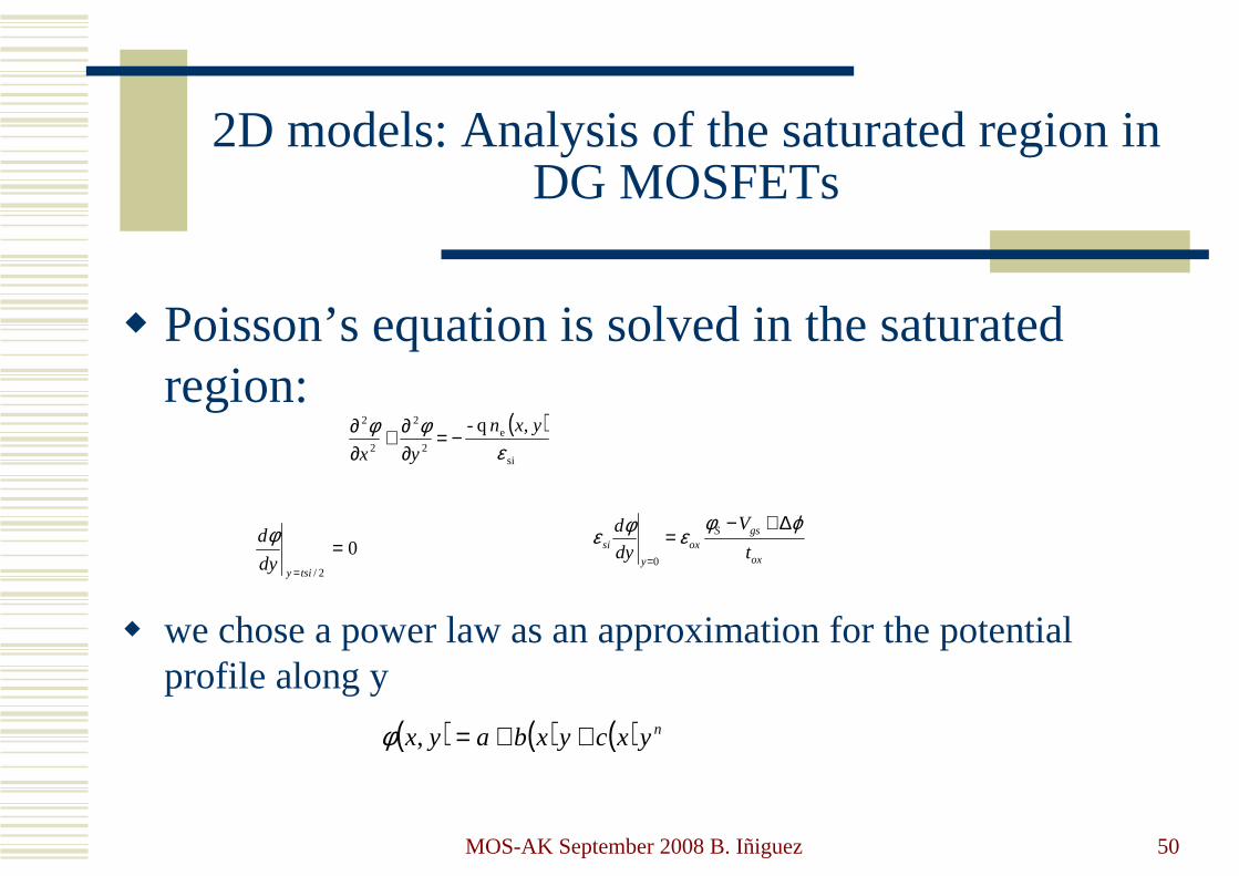
2D models: Analysis of the saturated region in DG MOSFETs
x
y
∆LS D
G
G
L
tsi
GCA region Saturation region
MOS-AK September 2008 B. Iñiguez 50
2D models: Analysis of the saturated region in DG MOSFETs
� Poisson’s equation is solved in the saturated region:
� we chose a power law as an approximation for the potential profile along y
( )si
e2
2
2
2 ,q-
εφφ yxn
yx−=
∂∂+
∂∂
( ) ( ) ( ) nyxcyxbayx ++=,φ
02/
== tsiy
dy
dφox
gsSox
y
si t
V
dy
d ϕφεφε
∆+−=
=0
MOS-AK September 2008 B. Iñiguez 51
2D models: Analysis of the saturated region in DG MOSFETs
( ) n
n
siox
FBgsS
si
ox
ox
FBgsS
si
oxS y
ttn
VVy
t
VVyx
12
,−
⋅+−
−+−
+=φ
εεφ
εεφφ
for 2sity ≤
( ) ( ) ( )nsi
n
siox
gsS
si
oxsi
ox
gsS
si
oxS yt
ttn
Vyt
t
Vyx −
⋅∆+−
−−∆+−
+=−1
2,
ϕφεεϕφ
εεφφ
for 2sity >
ox
FBgsS
si
ox
si
mtsi
t
VVQdy
x
+−+−=
∂∂∫
φεε
εφ
20
2
2Integrating:
Qm is considered constant in the saturated region
022
2
=−∂∂
λϕϕ
x
ox
mgsS C
QV
2−∆+−= ϕφϕ
( ) ( )1
1
2
1
2
1
21
21
82
2
+−+=
+−+=
nnr
t
nn
ttt sisi
ox
sioxsi
εελ
We have to solve in the x-direction:
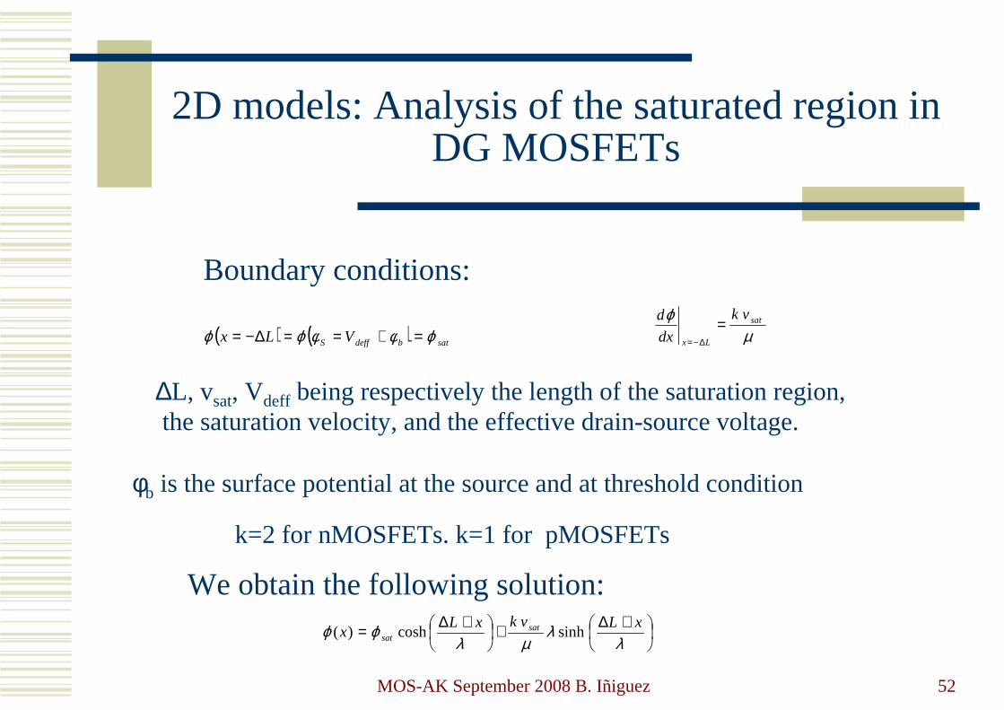
MOS-AK September 2008 B. Iñiguez 52
2D models: Analysis of the saturated region in DG MOSFETs
( ) ( ) satbdeffS VLx ϕφφϕϕ =+==∆−= µϕ sat
Lx
vk
dx
d =∆−=
Boundary conditions:
∆L, vsat, Vdeff being respectively the length of the saturation region,the saturation velocity, and the effective drain-source voltage.
φb is the surface potential at the source and at threshold condition
k=2 for nMOSFETs. k=1 for pMOSFETs
We obtain the following solution:
+∆+
+∆=λ
λµλ
ϕϕ xLvkxLx sat
sat sinhcosh)(
MOS-AK September 2008 B. Iñiguez 53
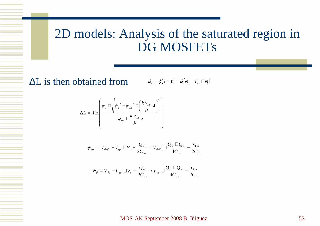
2D models: Analysis of the saturated region in DG MOSFETs
∆L is then obtained from ( ) ( )bdsSd Vx φφϕϕϕ +==== 0
+
+−+
=∆λ
µϕ
λµ
ϕϕϕλ
satsat
satsatdd
vk
vk
L
222
ln
ox
m
ox
msdeff
ox
mtgsdeffsat C
Q
C
QQV
C
QVVV
242−
++≈−+−=ϕ
ox
m
ox
msds
ox
mtgsdsd C
Q
C
QQV
C
QVVV
242−
++≈−+−=ϕ
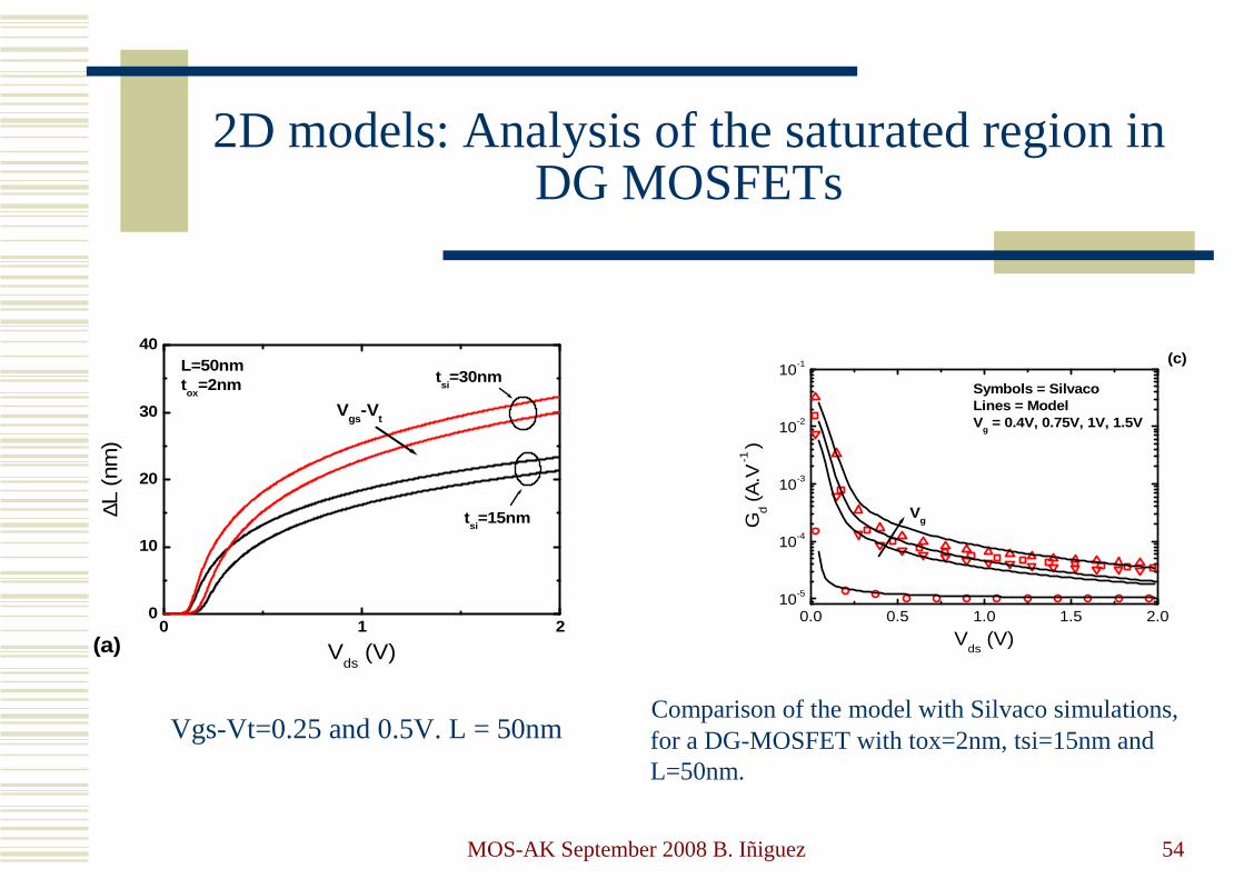
MOS-AK September 2008 B. Iñiguez 54
2D models: Analysis of the saturated region in DG MOSFETs
0 1 20
10
20
30
40
(a)
L=50nmtox
=2nm
tsi=15nm
tsi=30nm
Vgs
-Vt
∆L (
nm)
Vds
(V)
Vgs-Vt=0.25 and 0.5V. L = 50nm
0.0 0.5 1.0 1.5 2.010-5
10-4
10-3
10-2
10-1 (c)
Vg
Symbols = SilvacoLines = ModelV
g = 0.4V, 0.75V, 1V, 1.5V
Gd (A
.V -
1 )
Vds
(V)
Comparison of the model with Silvaco simulations,for a DG-MOSFET with tox=2nm, tsi=15nm andL=50nm.
MOS-AK September 2008 B. Iñiguez 55
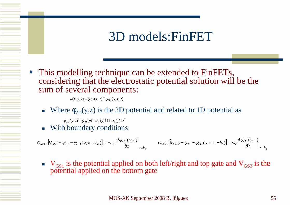
3D models:FinFET
� This modelling technique can be extended to FinFETs, considering that the electrostatic potential solution will be thesum of several components:
� Where φ2D(y,z) is the 2D potential and related to 1D potential as
� With boundary conditions
� VGS1 is the potential applied on both left/right and top gate and VGS2 is the potential applied on the bottom gate
),,(),(),,( 32 zyxzyzyx DD φφφ +=
2112 )()()(),( zyzyyzy oDD ⋅+⋅+= ααφφ
[ ]0
),(),( 2
211hz
DSioDmsGSox z
zyhzyVC
=∂∂−==−−⋅ φεφφ [ ]
0
),(),( 2
222hz
DSioDmsGSox z
zyhzyVC
=∂∂=−=−−⋅ φεφφ
MOS-AK September 2008 B. Iñiguez 56
3D models:FinFET
� φ1D(y) is the 1D potential solution:
� With boundary conditions:
� An analytical expression is found for φ1D(y)
tVyi
si
enq
y
y /)(2
2 )( φ
εφ
=∂
∂
0)(
0
1 =∂
∂
=y
D
y
yφ [ ]oty
sioDmsGSoxo ytyVC
=∂∂⋅−==−−⋅ 0
11 )(φεφφ
MOS-AK September 2008 B. Iñiguez 57
3D models:FinFET
� The 3D potential component is the solution of the remaining 3D Laplace’s equation with boundary conditions
� An analytical expression is found for φ3D
� The approximations used to obtain the analytical solution were to consider that:
� φF is constant along the channel (which is valid in subthreshold) and equal to its value at the source end of the channel
� the short-channel effects are not very severe, so that φ1D is the dominant potential contribution for the electron charge density
[ ]0
),,(),,(0 3
31hz
DSioDox z
zyxhzyxC
=∂∂
−==−⋅φ
εφ [ ]0
),,(),(0 3
22hz
DSioDox z
zyxhzyC
=∂∂
=−=−⋅φ
εφ
),(),,0( 23 zyVzy DbiD φφ −= ),(),,( 23 zyVVzyL DbiDSD φφ −+=
MOS-AK September 2008 B. Iñiguez 58
3D models:FinFET
� Using our analytical model for the electrostatic potential, we obtain ananalytical expression of the location of the virtual cathode (the point along the channel where the potential is minimum, and therefore, of the minimum value φmin
� The position of the virtual cathode will be instrumental to derive the subthreshold swing and threshold voltage expressions.
� Subthreshold swing and threshold voltage models can be developed by taking the values of the integrands at the conduction path (yc,zc)
MOS-AK September 2008 B. Iñiguez 59
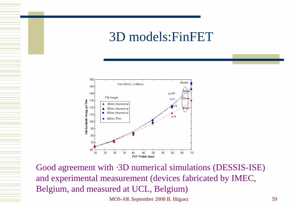
3D models:FinFET
Good agreement with ·3D numerical simulations (DESSIS-ISE)and experimental measurement (devices fabricated by IMEC, Belgium, and measured at UCL, Belgium)
MOS-AK September 2008 B. Iñiguez 60
3D models:FinFET
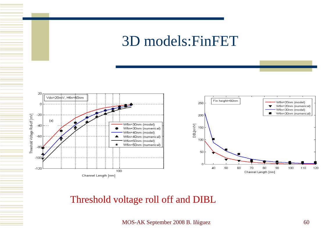
Threshold voltage roll off and DIBL
MOS-AK September 2008 B. Iñiguez 61
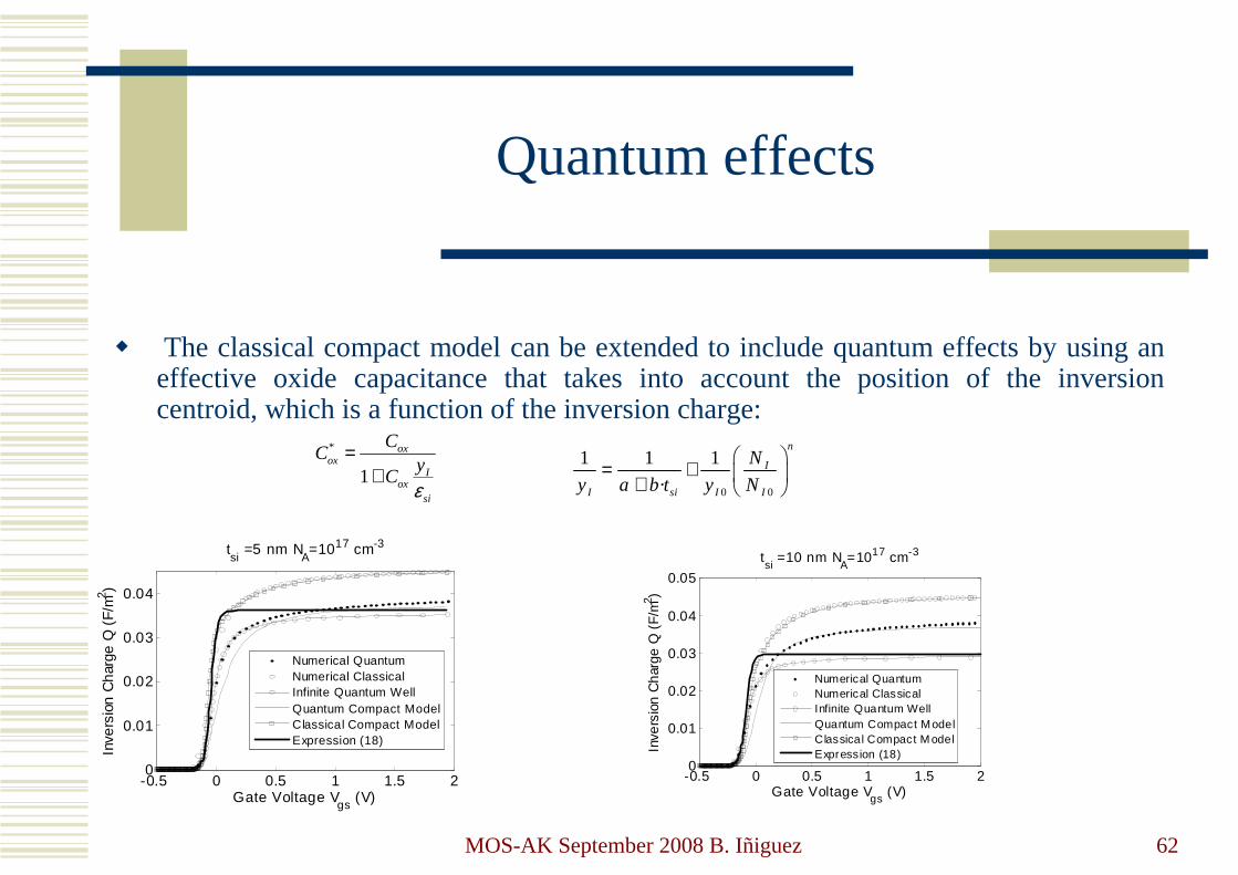
Quantum effects
� If the silicon layer in the DG and GAA MOSFETs is thinner than 10 nm, quantum confinement cannot be ignored, and Poisson’s equation should be solved self-consistently with Schrödinger’s equation.
� For this case, an analytical solution is not possible without making assumptions of either the shape of the potential distribution or of the electron distribution.
MOS-AK September 2008 B. Iñiguez 62
Quantum effects
� The classical compact model can be extended to include quantum effects by using an effective oxide capacitance that takes into account the position of the inversion centroid, which is a function of the inversion charge:
*
1
oxox
Iox
si
CC
yC
ε
=+
0 0
1 1 1
·
n
I
I si I I
N
y a b t y N
= + +
-0.5 0 0.5 1 1.5 20
0.01
0.02
0.03
0.04
Gate Voltage Vgs
(V)
Inve
rsio
n C
har
ge Q
(F
/m2 )
tsi
=5 nm NA=1017 cm-3
Numerical QuantumNumerical ClassicalInfinite Quantum WellQuantum Compact ModelClassical Compact ModelExpression (18)
-0.5 0 0.5 1 1.5 20
0.01
0.02
0.03
0.04
0.05
Gate Voltage Vgs (V)
Inve
rsio
n C
har
ge Q
(F
/m2 )
tsi
=10 nm NA=1017 cm-3
Numerical QuantumNumerical ClassicalInfinite Quantum WellQuantum Compact ModelClassical Compact M odelExpression (18)
MOS-AK September 2008 B. Iñiguez 63
Quantum effects
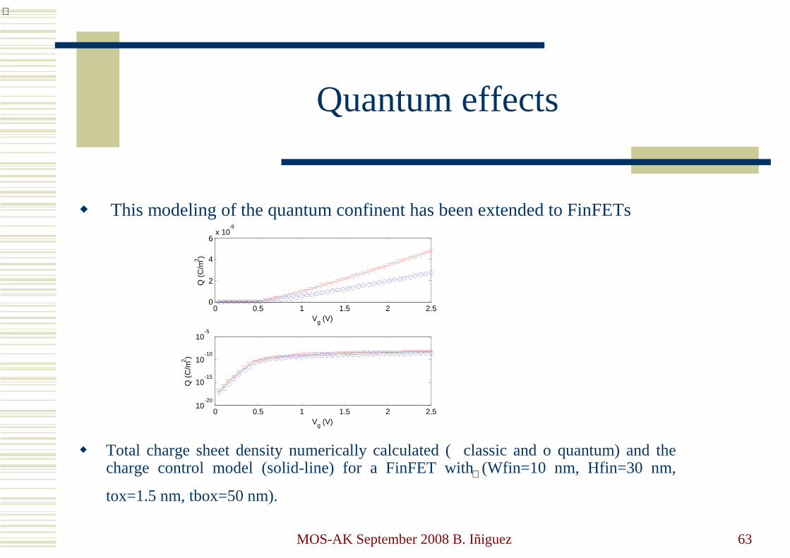
� This modeling of the quantum confinent has been extended to FinFETs
� Total charge sheet density numerically calculated ( classic and o quantum) and the charge control model (solid-line) for a FinFET with (Wfin=10 nm, Hfin=30 nm,
tox=1.5 nm, tbox=50 nm).
0 0.5 1 1.5 2 2.50
2
4
6x 10
-9
Vg (V)
Q (
C/m
2 )
0 0.5 1 1.5 2 2.510
-20
10-15
10-10
10-5
Vg (V)
Q (
C/m
2 )
∇
∇
MOS-AK September 2008 B. Iñiguez 64
Hydrodynamic model
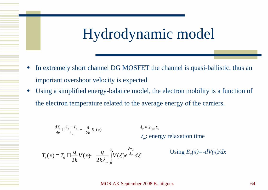
� In extremely short channel DG MOSFET the channel is quasi-ballistic, thus an
important overshoot velocity is expected
� Using a simplified energy-balance model, the electron mobility is a function of
the electron temperature related to the average energy of the carriers.
0 ( )2
e ex
w
dT T T qE x
dx kλ−+ = − wsatw v τλ 2≈
τw: energy relaxation time
0
0
( ) ( ) ( )2 2
w
yx
ew
q qT x T V x V e d
k k
ξλξ ξ
λ
−
= + − ∫UsingEx(x)=-dV(x)/dx
MOS-AK September 2008 B. Iñiguez 65
Hydrodynamic model
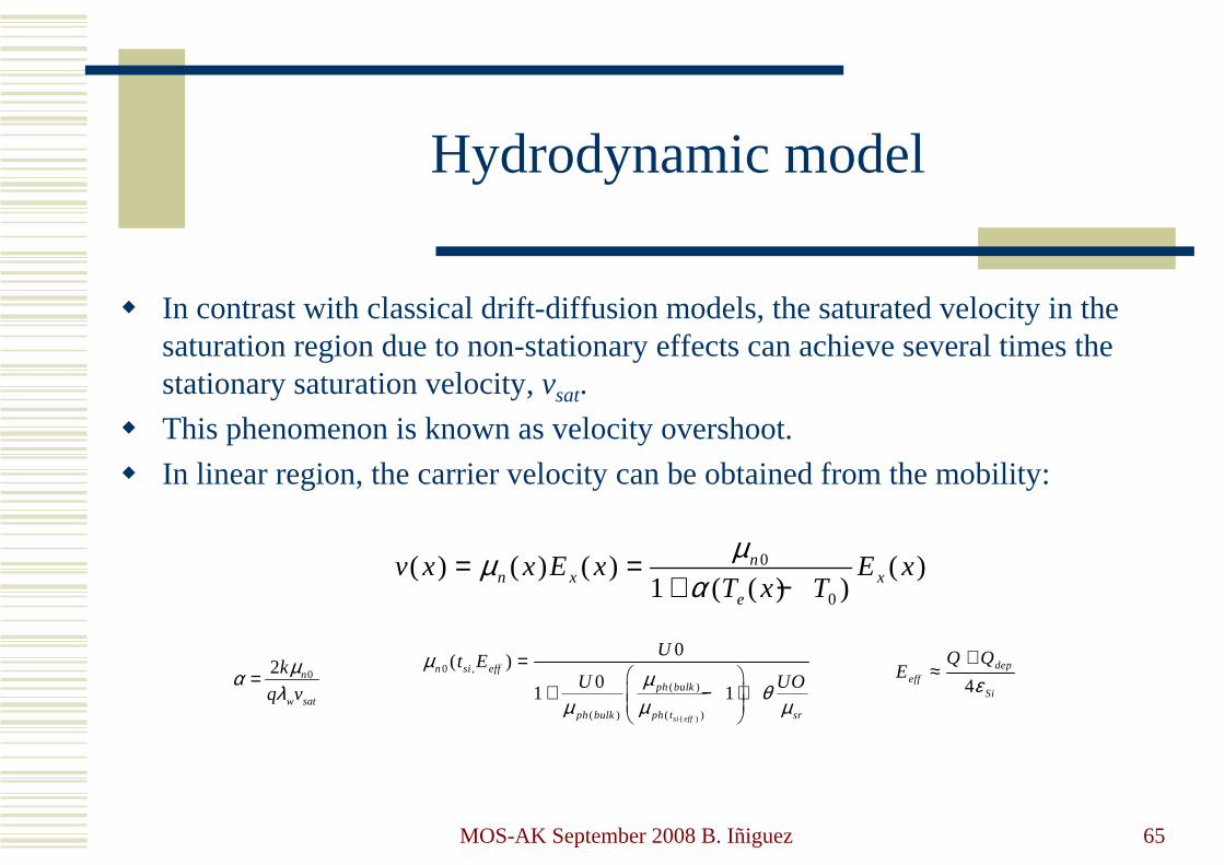
� In contrast with classical drift-diffusion models, the saturated velocity in the saturation region due to non-stationary effects can achieve several times the stationary saturation velocity, vsat.
� This phenomenon is known as velocity overshoot.
� In linear region, the carrier velocity can be obtained from the mobility:
0
0
( ) ( ) ( ) ( )1 ( ( ) )
nn x x
e
v x x E x E xT x T
µµα
= =+ −
02 n
w sat
k
q v
µαλ
=
( )
0 ,
( )
( ) ( )
0( )
01 1
si eff
n si eff
ph bulk
ph bulk ph t sr
Ut E
U UOµ
µθ
µ µ µ
=
+ − +
4dep
effSi
Q QE
ε+
≈
MOS-AK September 2008 B. Iñiguez 66
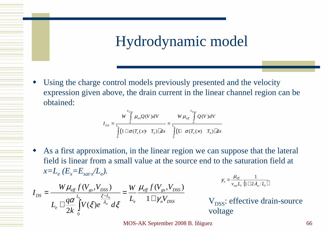
Hydrodynamic model
� Using the charge control models previously presented and the velocity expression given above, the drain current in the linear channel region can be obtained:
� As a first approximation, in the linear region we can suppose that the lateral field is linear from a small value at the source end to the saturation field at x=Le (Ex=Esat·x/Le).
( ) ( )
0
0 0
0 0
0 0
( ) ( )
1 ( ( ) ) 1 ( ( ) )
Dsat Dsat
e e
V V
n eff
DS L L
e e
W Q V dV W Q V dV
I
T x T dx T x T dx
µ µ
α α= =
+ − + −
∫ ∫
∫ ∫
0
( , ) ( , )
1( )
2
ee
w
eff gs DSS eff gs DSSDS LL
e n DSSe
W f V V f V VWI
L VqL V e d
k
ξλ
µ µγα ξ ξ
−= =+
+ ∫
( )ewesat
effn LLv λ
µγ
21
1
+=
VDSS: effective drain-sourcevoltage
MOS-AK September 2008 B. Iñiguez 67
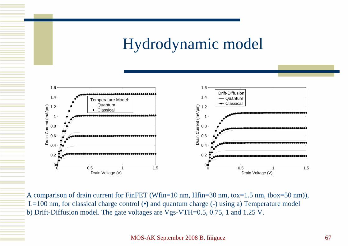
Hydrodynamic modelD
rain
Cur
rent
(m
A/µ
m)
Temperature Model: Quantum Classical
0 0.5 1 1.50
0.2
0.4
0.6
0.8
1
1.2
1.4
1.6
Drain Voltage (V)
Dra
in C
urre
nt (
mA
/µm
)
0 0.5 1 1.50
0.2
0.4
0.6
0.8
1
1.2
1.4
1.6
Drain Voltage (V)
Drift-Diffusion: Quantum Classical
A comparison of drain current for FinFET (Wfin=10 nm, Hfin=30 nm, tox=1.5 nm, tbox=50 nm)),L=100 nm, for classical charge control (•) and quantum charge (-) using a) Temperature model b) Drift-Diffusion model. The gate voltages are Vgs-VTH=0.5, 0.75, 1 and 1.25 V.
MOS-AK September 2008 B. Iñiguez 68
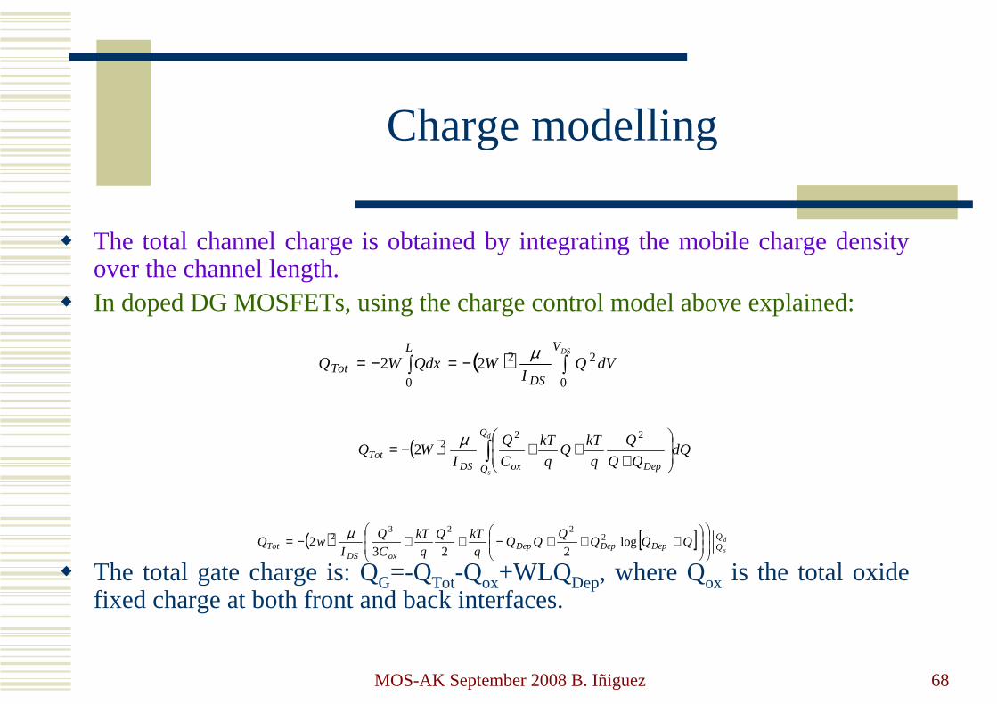
Charge modelling
� The total channel charge is obtained by integrating the mobile charge density over the channel length.
� In doped DG MOSFETs, using the charge control model above explained:
� The total gate charge is: QG=-QTot-Qox+WLQDep, where Qox is the total oxide fixed charge at both front and back interfaces.
( )∫ ∫−=−=L V
DSTot
DS
dVQI
WQdxWQ0 0
2222µ
( ) ∫
+++−=
d
s
Q
Q DepoxDSTot dQ
Q
q
kTQ
q
kT
C
Q
IWQ
2222
µ
( ) [ ] d
s
QQDepDepDep
oxDSTot QQQ
QQQ
q
kTQ
q
kT
C
Q
IwQ
+++−++−= log
2232 2
2232 µ
MOS-AK September 2008 B. Iñiguez 69
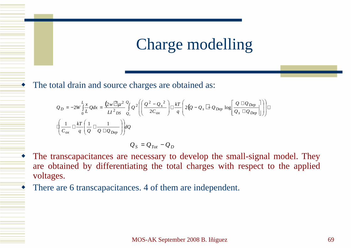
Charge modelling
� The total drain and source charges are obtained as:
� The transcapacitances are necessary to develop the small-signal model. They are obtained by differentiating the total charges with respect to the applied voltages.
� There are 6 transcapacitances. 4 of them are independent.
( ) ( )
dQQQQq
kT
C
QQQQQ
q
kT
C
QQQ
LI
wQdx
L
xWQ
Depox
Q
Q Deps
DepDeps
ox
s
DS
L
D
d
s
+++⋅
⋅
++
−−+
−=−= ∫∫
111
log22
22
222
2
23
0
µ
DTotS QQQ −=
MOS-AK September 2008 B. Iñiguez 70
Charge modelling
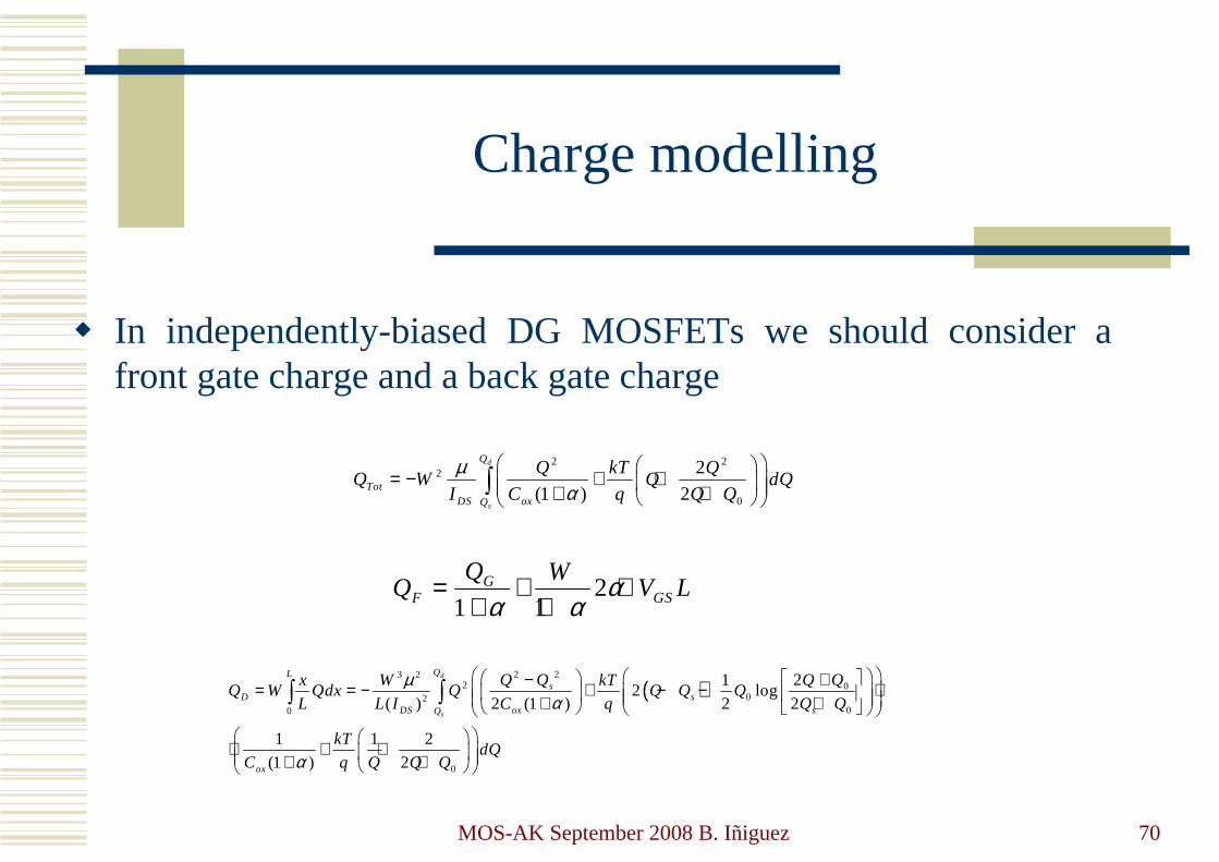
� In independently-biased DG MOSFETs we should consider a front gate charge and a back gate charge
21 1
GF GS
Q WQ V Lα
α α= + ⋅
+ +
2 22
0
2
(1 ) 2
d
s
Q
TotDS oxQ
Q kT QQ W Q dQ
I C q Q Q
µα
= − + + + +
∫
( )2 23 2
2 002
00
0
212 log
( ) 2 (1 ) 2 2
1 1 2
(1 ) 2
d
s
QLs
D sDS ox sQ
ox
Q Q Q Qx W kTQ W Qdx Q Q Q Q
L L I C q Q Q
kTdQ
C q Q Q Q
µα
α
− += = − + − − ⋅ + +
⋅ + + + +
∫ ∫
MOS-AK September 2008 B. Iñiguez 71
Charge modelling
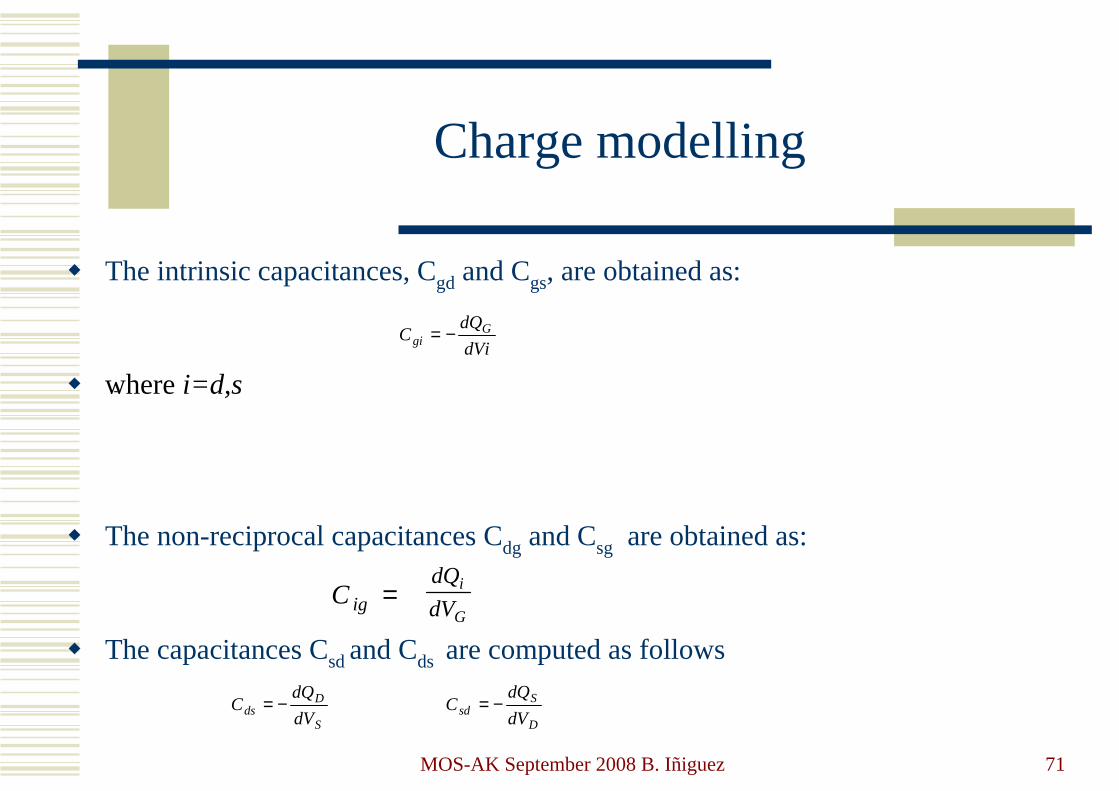
� The intrinsic capacitances, Cgd and Cgs, are obtained as:
� where i=d,s
� The non-reciprocal capacitances Cdg and Csg are obtained as:
� The capacitances Csdand Cds are computed as follows
dVi
dQC G
gi −=
-
=igCG
i
dV
dQ
S
Dds dV
dQC −=
D
Ssd dV
dQC −=
MOS-AK September 2008 B. Iñiguez 72
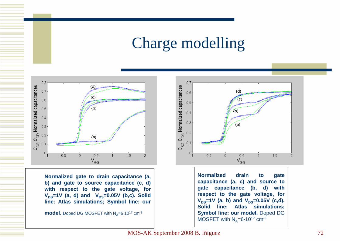
Charge modelling
-
Normalized gate to drain capacitance (a, b) and gate to source capacitance (c, d) with respect to the gate voltage, for VDS=1V (a, d) and V DS=0.05V (b,c). Solid line: Atlas simulations; Symbol line: our
model. Doped DG MOSFET with NA=6·1017 cm-3
Normalized drain to gate capacitance (a, c) and source to gate capacitance (b, d) with respect to the gate voltage, for VDS=1V (a, b) and V DS=0.05V (c,d). Solid line: Atlas simulations; Symbol line: our model. Doped DG MOSFET with NA=6·1017 cm-3
MOS-AK September 2008 B. Iñiguez 73
Charge modelling
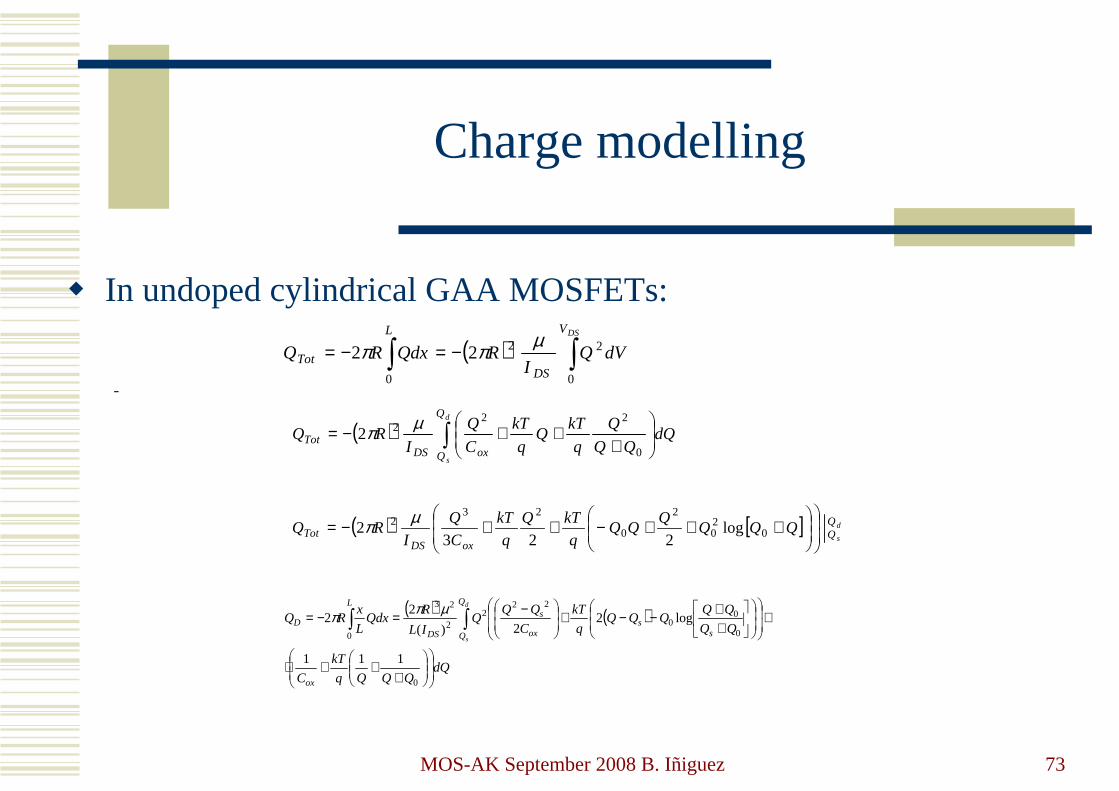
� In undoped cylindrical GAA MOSFETs:
-
( )∫ ∫−=−=L V
DSTot
DS
dVQI
RQdxRQ0 0
2222µππ
( ) ∫
+++−=
d
s
Q
Q oxDSTot dQ
Q
q
kTQ
q
kT
C
Q
IRQ
0
2222
µπ
( ) ( )
dQQQQq
kT
C
QQQQQ
q
kT
C
QQQ
IL
RQdx
L
xRQ
ox
Q
Q ss
ox
s
DS
L
D
d
s
+++⋅
⋅
++−−+
−=−= ∫∫
0
0
00
222
2
23
0
111
log22)(
22
µππ
( ) [ ] d
s
oxDSTot QQQ
QQQ
q
kTQ
q
kT
C
Q
IRQ
+++−++−= 0
20
2
0
232 log
2232
µπ
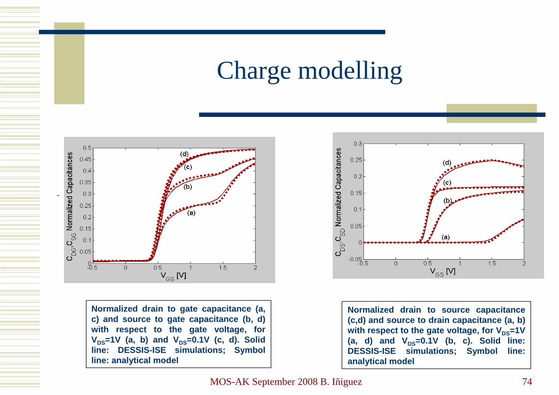
MOS-AK September 2008 B. Iñiguez 74
-
Charge modelling
Normalized drain to gate capacitance (a, c) and source to gate capacitance (b, d) with respect to the gate voltage, for VDS=1V (a, b) and V DS=0.1V (c, d). Solid line: DESSIS-ISE simulations; Symbol line: analytical model
Normalized drain to source capacitance (c,d) and source to drain capacitance (a, b) with respect to the gate voltage, for V DS=1V (a, d) and V DS=0.1V (b, c). Solid line: DESSIS-ISE simulations; Symbol line: analytical model
MOS-AK September 2008 B. Iñiguez 75
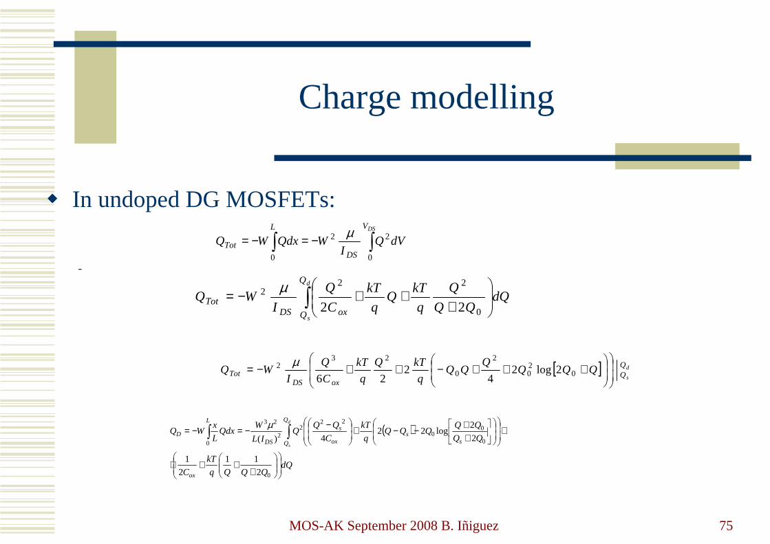
Charge modelling
� In undoped DG MOSFETs:
-
∫ ∫−=−=L V
DSTot
DS
dVQI
WQdxWQ0 0
22 µ
∫
+++−=
d
s
Q
Q oxDSTot dQ
Q
q
kTQ
q
kT
C
Q
IWQ
0
222
22
µ
( )
dQQQQq
kT
C
QQQQQ
q
kT
C
QQQ
IL
WQdx
L
xWQ
ox
Q
Q ss
ox
s
DS
L
D
d
s
+++⋅
⋅
++−−+
−−=−= ∫∫
0
0
00
222
2
23
0
2
11
2
1
2
2log22
4)(
µ
[ ] d
s
oxDSTot QQQ
QQQ
q
kTQ
q
kT
C
Q
IWQ
+++−++−= 0
20
2
0
232 2log2
42
26
µ
MOS-AK September 2008 B. Iñiguez 76
-
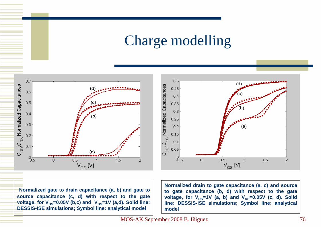
Charge modelling
Normalized gate to drain capacitance (a, b) and gat e to source capacitance (c, d) with respect to the gate voltage, for V DS=0.05V (b,c) and V DS=1V (a,d). Solid line: DESSIS-ISE simulations; Symbol line: analytical mod el
Normalized drain to gate capacitance (a, c) and sou rce to gate capacitance (b, d) with respect to the gate voltage, for V DS=1V (a, b) and V DS=0.05V (c, d). Solid line: DESSIS-ISE simulations; Symbol line: analytic al model
-0.5 0 0.5 1 1.5 20
0.05
0.1
0.15
0.2
0.25
0.3
0.35
0.4
0.45
0.5
CD
G,C
SG N
orm
aliz
ed C
apac
itanc
es
VGS
[V]
(a)
(d)
(c)
(b)
MOS-AK September 2008 B. Iñiguez 77
-
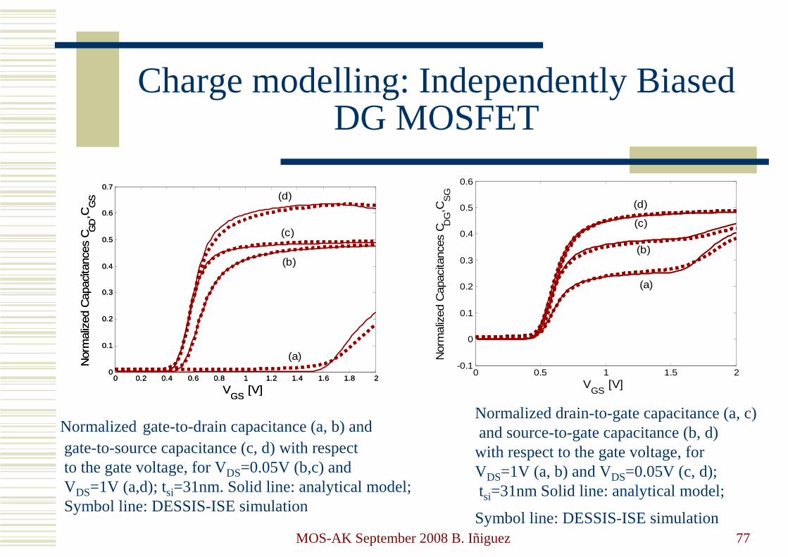
Charge modelling: Independently BiasedDG MOSFET
0 0.2 0.4 0.6 0.8 1 1.2 1.4 1.6 1.8 20
0.1
0.2
0.3
0.4
0.5
0.6
0.7
Nor
mal
ized
Cap
acita
nces
CG
D,C
GS
VGS
[V] 0 0.2 0.4 0.6 0.8 1 1.2 1.4 1.6 1.8 2
0
0.1
0.2
0.3
0.4
0.5
0.6
0.7
Nor
mal
ized
Cap
acita
nces
CG
D,C
GS
VGS
[V]
(c)
(b)
(a)
(d)
0 0.5 1 1.5 2-0.1
0
0.1
0.2
0.3
0.4
0.5
0.6
Nor
mal
ized
Cap
acita
nces
CD
G,C
SG
VGS
[V]
(a)
(d)
(c)
(b)
Normalized gate-to-drain capacitance (a, b) andgate-to-source capacitance (c, d) with respectto the gate voltage, for VDS=0.05V (b,c) and VDS=1V (a,d); tsi=31nm. Solid line: analytical model;Symbol line: DESSIS-ISE simulation
Normalized drain-to-gate capacitance (a, c)and source-to-gate capacitance (b, d) with respect to the gate voltage, for VDS=1V (a, b) and VDS=0.05V (c, d);tsi=31nm Solid line: analytical model;
Symbol line: DESSIS-ISE simulation
MOS-AK September 2008 B. Iñiguez 78
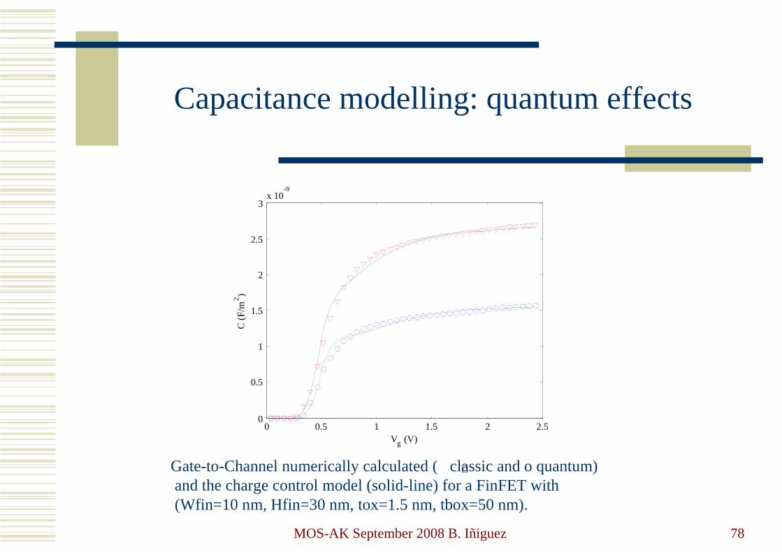
Capacitance modelling: quantum effects
0 0.5 1 1.5 2 2.50
0.5
1
1.5
2
2.5
3x 10
-9
Vg (V)
C (
F/m
2 )
Gate-to-Channel numerically calculated ( classic and o quantum)and the charge control model (solid-line) for a FinFET with(Wfin=10 nm, Hfin=30 nm, tox=1.5 nm, tbox=50 nm).
∇
MOS-AK September 2008 B. Iñiguez 79
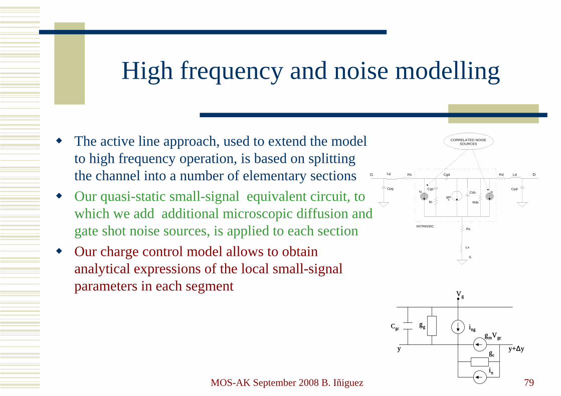
High frequency and noise modelling
� The active line approach, used to extend the modelto high frequency operation, is based on splittingthe channel into a number of elementary sections
� Our quasi-static small-signal equivalent circuit, towhich we add additional microscopic diffusion andgate shot noise sources, is applied to each section
� Our charge control model allows to obtainanalytical expressions of the local small-signalparameters in each segment
y y+∆y
Cgcgg ing
gc
gmV gc
in
Vg
y y+∆y
Cgcgg ing
gc
gmV gc
in
Vg
Cpg
Lg
Cgs
Cgd
Ri
gmτ
Rs Rd Ld
CpdCds
Rds
Rs
Ls
G D
INTRINSIC
S
id
CORRELATED NOISESOURCES
ig
MOS-AK September 2008 B. Iñiguez 80
High frequency and noise modelling
� In order to model noise using this technique, several approacheshave been considered:� The contribution to noise of the length where carriers travel at
the saturation velocity must not neglected.
� A Diffusion Coefficient is used to define the microscopicnoisecurrent sources, in order to consider the short channel effect. Theexpression of the diffusion coefficient is valid from low tohighfields
� Mobility reduction should be considered along the channel.
MOS-AK September 2008 B. Iñiguez 81
High frequency and noise modelling
� The active transmission line is analysed using the nodal admittance method� Once the intrinsic admittance matrix, Yi, and admittance correlation matrix, CYi, are
obtained, extrinsic elements are included� Thermal noise is considered for access resistances� Gate tunnelling current, and its associated shot noise source are added
� Using the model, we calculate the S-parameters and the usual noise parameters: Fmin, Rn (equivalent noise resistance) and Gopt (optimum reflection coefficient)
�
MOS-AK September 2008 B. Iñiguez 82
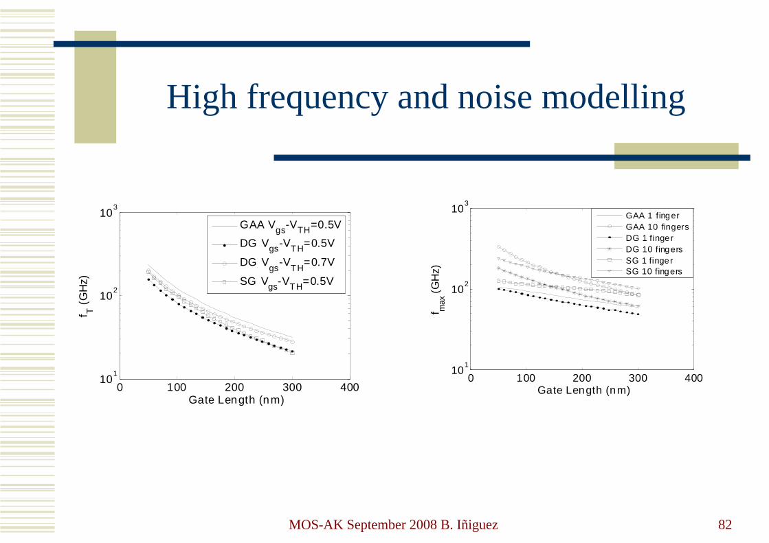
High frequency and noise modelling
0 100 200 300 40010
1
102
103
Gate Length (nm)
f T (
GH
z)
GAA Vgs-VTH=0.5V
DG Vgs-VTH=0.5V
DG Vgs
-VTH
=0.7V
SG Vgs-VTH=0.5V
0 100 200 300 40010
1
102
103
Gate Length (nm)
f max
(G
Hz)
GAA 1 fingerGAA 10 fingersDG 1 fingerDG 10 fingersSG 1 fingerSG 10 fingers
MOS-AK September 2008 B. Iñiguez 83
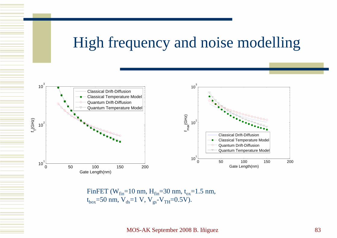
High frequency and noise modelling
0 50 100 150 20010
1
102
103
Gate Length(nm)
f T(GH
z)
Classical Drift-DiffusionClassical Temperature ModelQuantum Drift-DiffusionQuantum Temperature Model
FinFET (Wfin=10 nm, Hfin=30 nm, tox=1.5 nm, tbox=50 nm, Vds=1 V, Vgs-VTH=0.5V).
0 50 100 150 20010
1
102
103
Gate Length(nm)
f max
(GH
z)
Classical Drift-DiffusionClassical Temperature ModelQuantum Drift-DiffusionQuantum Temperature Model

MOS-AK September 2008 B. Iñiguez 84
High frequency and noise modelling
20 40 60 80 100 120 140 1600
0.5
1
1.5
2
2.5
3
Gate Length(nm)
Fm
in(d
B)
Extrinsic Noise Figure
Classical Drift-DiffusionClassical Temperature ModelQuantum Drift-DiffusionQuantum Temperature Model
FinFET (Wfin=10 nm, Hfin=30 nm, tox=1.5 nm, tbox=50 nm, 100 fingers, Vgs-VTH=0.5V, Vds=1V)
0 20 40 60 80 1000
1
2
3
4
5
6
7
Frequency (GHz)
F min
(dB
)
Classical Drift-DiffusionClassical Temperature ModelQuantum Drift-DiffusionQuantum Temperature Model
Extrinsic
Intrinsic
MOS-AK September 2008 B. Iñiguez 85
Conclusions
� We have discussed techniques to develop compact models in Thin-Film SOI MOSFETs(FD SOI MOSFDETs, AM SOI MOSFETs, DG MOSFETs, GAA MOSFETs, FinFETs)
� Very few models are currently available for FD SOI MOSFETs in circuit simulators� No models available for AM SOI MOSFETs� Compact models for Multi-Gate MOSFETs are still under development
� They face important challenges for nanoscale devices: scaling with volumeinversion/accumulation, quantum confinement, hydrodinamic transport
� These effects, although considered by UFDG, are hard totake into account in a full compact analytical way
MOS-AK September 2008 B. Iñiguez 86
Conclusions
� We have also reviewed our approaches:� A core model, developed from a unified charge control model obtained from the 1D
Poisson’s equation (using some approximations in the case of DG MOSFETs)� 2D or 3D scalable models of the short-channel effects (threshold voltage roll-off, DIBL,
subthreshold swing degradation and channel length modulation), developed by solvingthe 2D or 3D Poisson’s equation using appropriate techniques
� Quantum effects have been including by using an effectiveoxide thickness whichaccounts for the position of the inversion centroid
� The active transmission line approach extends the models to the high frequency andnoise analysis